| Posted By

SukkoPera
on 2022-10-30
15:08:07
|  New Project: Hannes-compatible 256k RAM Expansion New Project: Hannes-compatible 256k RAM Expansion
Another thing I've been working on recently is a solderless Hannes-compatible 256k RAM expansion for the C16.
I started from Solder's notes, figured out the logic behind it and reimplemented everything in a GAL. I also tried to find an alternative to the MOS 6529 he used and ended up replacing it with two 74x74's and a 74x245. The latter is required in order to make the RAM register readable, which is something I had initially overlooked (and I'm still unsure why programs need to read it but oh well), so I had to hack that back in, which I will now need to integrate properly into the design. Yeah, it's three chips vs. one but the "usual" replacements do not work in this case because they all miss one feature of the original 6529 that is generally negligible but that is essential in this design: the fact that outputs are high after power-up/reset.
Other than that, everything seems to be working OK, even though I haven't been able to find a proper way of testing it. What I can say at the moment is that Mega Assembler and Taurin detect the 256k. The former starts up while the latter doesn't, but it might be due to a SD2IEC-incompatible loader.

I saw a video from siz I think, where he seems to have a proper RAM testing program but I haven't been able to find that anywhere. Would you please be willing to share it?
If the project works as it should, I will release it openly under CC-BY-NC-SA as usual. If it doesn't, I'll ask for help and we'll make it work somehow  . .
One thing I still don't know is whether the board will physically fit under the keyboard in the C16 or not, but I'm sure it won't on the Plus/4. But once it works, we can come up with something suitable :).
|
|
Posted By
TLC
on 2022-10-30
19:36:30
| Re: New Project: Hannes-compatible 256k RAM Expansion
I have been also playing around with cleaning up Hannes' / Solder's design in the last couple of years (time to time coming back to the thing). I didn't make it solderless, I merely wanted to clean up the mess imposed by the original design (i.e. piggybacking). So, I kept the classic RAM bank replacement method, and put the control logic on a single daughterboard that plugged into a precision socket in the place of the $FD10 6529B. A soldered-in wire harness connected to the board, and collected the required extra signals. (This was all obviously for the Plus/4.) Of course I have experimented with it a lot. The last prototype also added Csory expansion logic compatibility. (I have decided to drop that, however, from the next prototype... as I found out, the schema is just marginally supported. In practice I have also found the combined Hannes / Solder / Csory thing somewhat less than optimal as per complexity vs. functionality... all in all, finally I became less than enthusiastic about it so it will be dropped.) I have also planned to move the thing to GALs in the next prototype, to reduce size and complexity (not done yet).
Theoretically, at least 4 bits need to be implemented from the $FD16 page register (--> two function select bits and two page select bits). For full compatibility, however, I guess implementing a full 8-bit page register is required. (The extra 4 bits are functionally redundant. Yet, running Hannes/Solder compatible code, given the original design's 6529B, I think rightfully expects a full 8-bit read-writeable register at $FD16. The absence of the "unused" 4 bits may, or may not cause problems in practice, given arbitrary code.) BTW speaking of why "reading" the page register is needed in the first place (with or without implementing every bits), I seem to remember some Hannes/Solder expansion detection logic to rely on finding out whether the $FD16 register existed (at all) first, and if it did, finding out whether it was identical (or, separate) to the $FD10 register.
To first test the thing, I think Synergy's old 256k Support specific demos are perfect. Future World and Dream World come to mind first. Taurin can be also a good candidate. Yep, these old stuffs typically use specific loaders (unlikely to cooperate with an sd2iec).
With regards to a C16 compatible, 41256 based ram expansion design, I suspect, current consumption could be a factor.
|
|
Posted By
siz
on 2022-11-01
16:24:03
| Re: New Project: Hannes-compatible 256k RAM Expansion
@SukkoPera: I think my memory test was linked somewhere on the forum before. You can find it here: http://siz.hu/external/memory_test.prg
I like these rebuild projects (to an extent). But in this specific case the 6502 plus 4 approach seems better in every aspects: size, energy consumption, etc. It's a single board carrying a 6502, an FPGA for replacing the CPU port and emulate RAM banking register beside a single 512k x 8bit SRAM. It plugs in the CPU socket and is low enough to fit into a plus/4. You have to use only one external signal from the motherboard: the CAS.
|
|
Posted By
SukkoPera
on 2022-11-02
06:24:36
| Re: New Project: Hannes-compatible 256k RAM Expansion
@TLC: Well, making it solderless wasn't one of my goals, but the mod is more complex on the C16, as for instance it has 2x4416 RAM chips rather than 8x4164 like the +4, so it made sense to put everything on a single pluggable board and just pick up the few required signals that aren't available on the TED socket (and I was quite surprised to realize it gets no /RESET, I had never noticed!).
I was thinking about adding Csory compatibility at a later stage, but if you say so, I won't be doing that either. The "256k Support" tag in the Software sections seems to suggest that most software went for the Hannes method, so I guess it just makes sense to stick to that.
If you have a GitHub account I can add you as a project collaborator, so that maybe you can recycle my GAL work into your project. BTW, I just don't feel confident enough to open the project to the general public, but whoever wants to join is welcome, just ask, all you need is a GitHub account  . .
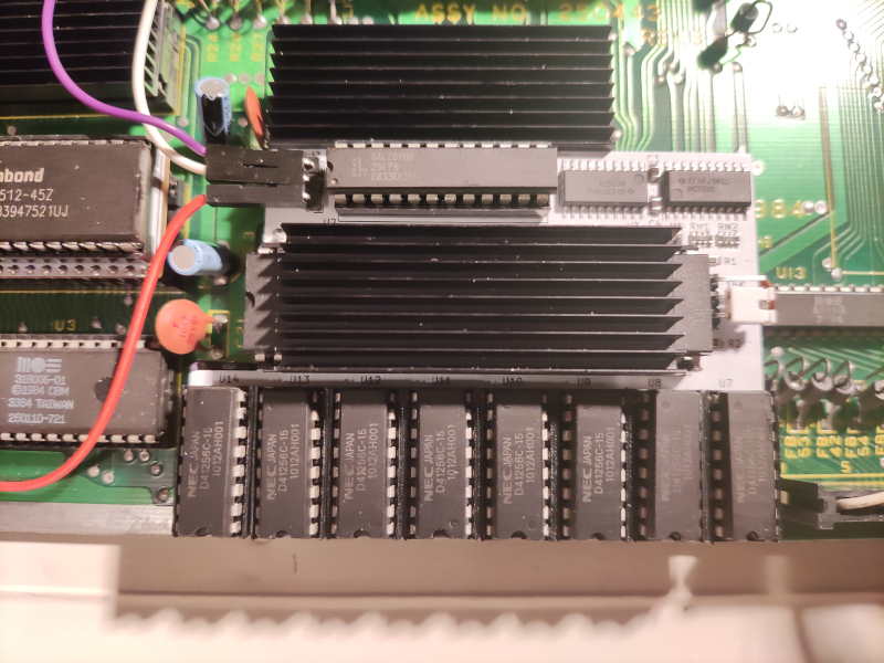
My solution currently implements only those 4 used bits of the $FD16 register. You should be able to see the 4 blobbed pins on the makeshift 245 in my pictures, which means the unused bits will always read as 1 . My solution is quite space-constrained (not counting the TED, there are 13 chips on that board!) and I really hope this will do, as adding the 74x245 is already quite a bit of a challenge. I guess another goal of my testing with this prototype will be to understand if that can be a problem or not. I have some ideas for the implementation of a full 8-bit register, but all require more chips, sigh.
I was convinced that software wouldn't need to read back the register, as the programmer always knows what to write there and there's nothing changing it behind the scenes. I was expecting detection routines to just write some value at some location, doing a blind bank switch and checking if it's still there, repeated a few times. But well, I guess I was wrong .
Yeah, power consumption can be a problem. I will have to do some checks about that.
@siz: Thanks for sharing your test program, I hadn't been able to find it. It detects the 256kB and all tests seem to pass, at least I get the same output as in your video, which makes me happy!
If you consider the effort, power consumption, size, I agree that the 6502plus4 is definitely better, but I think my approach has its own advantages, too: first, I learned a lot! And it was fun, too! Solder left docs on how to build the expansion but I had to reverse engineer how it works, think about how it could be replicated using the least amount of chips possible, come up with a 6529 replacement, write GAL equations, etc. It also helped me understand something about internal memory organization and refresh, since I was planning to do it with 2x4464 chips but then figured out it wouldn't work and why . This might seem trivial for hardware hackers, but I come from the software world and it really was an interesting experience to me.
Second: it allows me to test a circuit that I can later integrate into my LittleSixteen replacement mainboard.
Third: it is cheap. If you have a soldering iron and some soldering ability, you can probably build one for around 10-12€.
Fourth: it allows using the original CPU. I like the ability to replace the custom chips, but I also like to use the original hardware whenever possible.
... And when that is no longer possible, I would like the replacements to be open, which the 6502plus4 is not (to my knowledge). Any reimplementation can always introduce sneaky bugs, I like the idea that anybody can inspect the SW/HW and locate and fix them anytime. In fact, my project will be open, which paves the way to even more advantages besides that:
The schematics, PCB, GAL equations will be available for everyone to study, hopefully helping other people learn just as much as I did.
Openness means anyone can also improve the project: maybe someone with the required knowledge will come by and reimplement all the logic on a single CPLD/FPGA.
Another bonus is persistence over time: when Lotharek gets tired of selling the 6502plus4, there will be no more. We have already seen this with BSZ's SIDcard: it is an excellent piece of hardware, but he's selling the last examples. If someone will want to buy one next year, they won't be able to. Open projects will always be there for everyone to build, possibly adapting them to newer technology (say: replace a component if it's no longer available).
|
|
Posted By
siz
on 2022-11-02
10:10:33
| Re: New Project: Hannes-compatible 256k RAM Expansion
I agree with most of your points.
The main reason behind discountinuing the BSz SIDCard is the unavailability of the used CPLD/FPGA (I don't know which). He should redesign the card for a new component and that would be too much work.
Behind the scenes I also started to do a reimplementation of the Hannes memory expansion several years ago but didn't had the time to actually build it. I based it on an FPGA and an adapter which plugs into TED socket and also adds ROM expansion support with a 512k flash ROM that can contain 32 16k ROM images and any of them can be mapped to any of the 8 ROM banks (including BASIC ROM and KERNAL) with inplace flashing of images with a plus/4 program.
But that's a completely different story and since then the FPGA used in that design is also discontinued.
|
|
Posted By
TLC
on 2022-11-03
09:27:51
| Re: New Project: Hannes-compatible 256k RAM Expansion
@SukkoPera: I think I can see your points .
Yep, the TED has no Reset' (...BTW, it has no reset similarly to the 6529B, which IMHO made that chip quite less than ideal to be used as a page register - upon reset, the expanded memory page and config remain intact, LoL  - but that's another story). - but that's another story).
As for Csory compatibility, I wouldn't talk anyone either into or off from implementing it, I just made "my own" decision. (I'll write about that later.)
Yes, most stuffs actually support the Hannes/Solder schema. (Some years ago I checked quite a number of expanded memory specific stuffs about what schema they really supported. Unfortunately I didn't make notes about it - I was merely looking for one single true Csory memory expansion compatible stuff for testing "my" memory expansion controller prototype. All in all - I plan to repeat the test someday, and now record the results here.)
I prefer gitlab, but I also have a github account (let's discuss this later / in PM). Speaking of GAL equations, I think I already have that part ready, maybe I should share it. (Long story short - some months ago I felt inspired, and figured out that maybe I could fit the whole Hannes/Solder controlling logic, 8-bit read-writeable register included, into two 22V10 GAL's. I've already written the equations that compile successfully with galasm, but haven't tested the thing in practice, yet).
Maybe, omitting some or all unused bits from $FD16 (tying them to '1' just as you did) won't have such a big impact in practice that I presumed, who knows. (There aren't that many 256k-capable stuffs out there in the first place. Also, suppose that someone had either an enhanced, say, 512k or larger Hannes/Solder memory expansion, or, the Csory schema (whose enable bits are also in $FD16), then any legacy "256k Hannes/Solder" specific code "unprofessionally" fiddling with the unused 4 bits of the $FD16 register would already get into trouble anyway. Maybe it's indeed a legal expectation from Hannes/Solder/Csory aware programs to keep the "unused" bits "1" all the time, in which case, implementing the unused bits can indeed be omitted just as you did.)
Just for curiosity, this was my last prototype and layout below. No programmable logic chips there, they are all standard 74xx. The page register was built from a '574 and a '245 pair, with some additional controller logic. High-bits-on-reset was faked with weak pull-up resistors, plus a '74 that controlled the '574's OE' (Reset' disabled / first write to $FD16 enabled it). The register is not a full 6529B implementation, it couldn't be used as an input port (OTOH, at least it has valid Reset' ) , but it was perfect for the purpose. The prototype also already did implement the Csory expansion logic, ...minus a pair of inverters, because, I apparently got something wrong, and had to patch the thing later. All in all, the thing obviously grew a bit too large, and that was when I started to look for alternatives.


|
|
Posted By
MCes
on 2022-11-03
14:42:32
 | Re: New Project: Hannes-compatible 256k RAM Expansion
May I propose another time a GAL based solution for replacing the 6529B?
GAL22V10 reset all FF during power up ($0), FF are used for storing the inverted datas so at power up the output data will be $F (all output with collectors open).
In this application the open collector features and the relative pull-up resistors can be eliminated,
without the time-indetermination on 6529b inputs: the '573 can be used always as "transparent", so it can be replaced by a '244, '245, '541......
Some gal in / out pins remain free to be well used, especially if only the used register bits will be implemented.
A "reset on power up" is implemented into the GAL HW, but it can be also a input pin that can be connected to /RST line making the register resettable pushing the RESET button....
|
|
Posted By
TLC
on 2022-11-04
11:24:23
| Re: New Project: Hannes-compatible 256k RAM Expansion
@SukkoPera addendum (re: Csory memory expansion); as said whether someone feels enthusiastic about the Hannes / Solder / Csory memory expansion schema isn't really my business (...I know I definitely used to be ), yet, maybe it's worth writing down why "I" am already not.
In a nutshell, the Csory schema lets the programmer select one of four 16K windows of the CPU's 64K address space for paging. Then, 16K pages of the 256K expanded memory can be selected to appear in the selected address space window. The thing works transparent to the Hannes/Solder memory expansion. (That is, everything under Hannes/Solder remains as-is, except for the 16K window selected under the Csory expansion schema.) Also, the enable bits of the extension logic are in the Hannes/Solder control / page register i.e. $FD16.
At first sight, the "16K page in a selectable 16K window" approach is IMHO definitely much more elegant for the job than how the Hannes/Solder is doing it. Still...
My loss of enthusiasm started from the point where I realized the obvious, i.e., that there's no Csory expansion without a Hannes/Solder part implemented first. That is, what I have to judge is in fact not the Csory expansion itself, but inherently the combined bunch of the two in one. From that on, things IMHO take a bit different route, especially if resources are scarce (...which they are, as long as no modern PLDs are in the picture). First and most of all, from the point of adding the Csory extension, the basic function (i.e. memory paging) is literally implemented "twice"; that is, our thing is redundant, which is (by definition) a waste of resources. I'm just referring to my prototype above - the Csory extension AFAIR required four or five extra TTL gates to be added, which is a comparable number to the overall chip count of my previous (Hannes/Solder) controller prototype. Not only is the thing redundant, but (due to the alternative functions) the two need to be multiplexed together, which has also nothing to do with basic functionality (i.e. memory paging).
(When I think over what could have been implemented in roughly the same complexity of the Hannes/Solder memory controller's (let alone Hannes/Solder/Csory), I also find that the existing construct is suboptimal. The Hannes/Solder already has too many "control bits", "modes", "exceptions", if you please (implementing these exceptions takes resources comparable to that of basic paging functionality). I mean these "modes" IMO merely attempt to patch a conceptually flawed design (--> the design choice of paging ram in 64K long pages), and the implementation of the exceptions takes resources that don't serve basic i.e. memory paging functionality. ...Let alone Hannes/Solder/Csory, where just activating the Csory schema part starts off with wasting 2 potential address bits from the Hannes/Solder page register. If someone had said instead, hey, let's just start over from scratch, create two page registers of 4...8 bits each, assign them to the $4000-$7FFF and $8000-$BFFF address windows respectively, and let them both page in 16K pages of a 256K... theoretically up to 4M expanded memory space, the task would have been solved with practically no "function control" bits and corresponding overhead (all of them waste) at all. That is, we'd just have memory paging functionality superior to that of either Hannes/Solder, Csory, or both (...hey, we'd have two, clean, symmetric and completely independent page reigsters and pages!), in roughly equal (or even less) controller complexity. (*Reset for the page registers could have been somewhat tricky, but that's all.))
At that point, the Csory expansion could still have had some historical value (Csory has been a talented and very prolific guy IMHO), but when I started to look around finding releases for testing my prototype card, I found out that there were almost none. Most of the 256K specific programs, as previously said, speak Hannes/Solder. The rest, although not documented yet (my bad), mostly turned out to be HX-256 specific. I could find exactly two Csory specific programs. The first one is the Bard's Tale III Csory 256K release, which turned out to be buggy (...traced the culprit down to a small code snippet in the loader, no doubt it would never run on a true 256K capable config). The second is Csory's infamous 256K Macro Assembler, which I happened to have from someone. That stuff exclusively runs off a 32K ROM, which is fine, but it also requires committing the extra ROM hack loosely described in Solder's ROM expansion schematics, which is/was IMHO not. By then I was less than enthusiastic about raising my stakes, so I just didn't.
That's probably all about "my" story. Being a TTL junkie (and, when not, still very much preferring contemporary components with regards to old gear), I thought I'd just drop this from my next prototype (especially given that I might, as said, probably just get away with using two 22V10's, given I'd only implement the Hannes/Solder schema). No doubt there could be other considerations.
|
|
Posted By
SukkoPera
on 2022-11-07
05:23:39
| Re: New Project: Hannes-compatible 256k RAM Expansion
@MCes: I appreciate your help but I don't think I could fit that on my current board. Even if I could do that, I wouldn't be able to write the GAL equations for registered mode. If you want to do that, I offer my help to develop a new standalone 6529 replacement, I can work on the PCB and help with the testing.
@TLC: I see your point. For me it was like: if I want to add Csory compatibility it will take more logic; since I already have a lot to test, I will look into that later (if ever). Besides that, I had a look at what software supported both expansions and, as you said, most stuff works with Hannes.
But as you might have also noticed, there isn't much 256k-compatible software at all. I think this is in part due to the complexity of the programming model and part due to the scarce availability of ready-made expansions: the 6502plus4 is nice but rather expensive and it's more of a CPU replacement (and I'm not sure how hard it is to set it up so that the extra RAM is useable, does it need desoldering of the internal RAM?). I don't think anybody with a working CPU would buy it just for the 256k. Is there any other expansion? I hope my own will change that, at least, then it will be up to the developers to make new software .
|
|
Posted By
TLC
on 2022-11-07
18:37:51
| Re: New Project: Hannes-compatible 256k RAM Expansion
@SukkoPera : yep, the rarity of 256K specific programs generally goes back to the relative rarity of 256K equipped machines... which, in turn, goes back to the fact that all existing 256K(+) memory expansions require(d) installation work to be performed inside the machine. (Also, most 256K aware stuffs date back to the early-to-mid '90s, when the only way to have your machine expanded to 256K was via the tedious piggyback method described in Solder's contemporary document.) BTW, it's interesting but I can't see that many expanded memory aware programs for the C64 either, despite the fact that they had at least two widely supported and external memory modules available. (The 1764 REU has been a factory supported / official memexp module for the C64 / C128, and there has been also the GeoRam, which, albeit not as smart as a REU, is/was still pretty useable... and - unlike on Plus/4 - anybody could just get / plug in / use one.) Maybe there just hasn't been that much interest in creating 256K aware programs, except for a few specific fields (especially tools).
|
|
Posted By
SukkoPera
on 2023-03-17
19:42:39
| Re: New Project: Hannes-compatible 256k RAM Expansion
@TLC: Right. And until Sonic for the C64 came out, REUs could be bought for relatively cheap on eBay, sigh  . .
@MCes: I have been trying to write the registered mode equations and I think I made it. There is a slight problem though: The GAL22 only has an asynchronous reset input, the preset is synchronous. Since we need it to be asynchronous, we can use the reset, start with all 0s and always store and output the inverse of the input. The "other GAL" will need to handle that (easy in this scenario, not really in a generic 6529 replacement). A 74HCT240 can be used to provide the correct readback.
Is that what you implied when you said "inverted data"? I think it would work, but still I don't think I can fit it on my board :(.
|
|
Posted By
TLC
on 2023-03-17
07:20:31
| Re: New Project: Hannes-compatible 256k RAM Expansion
A late note, addition, whatever, to this topic...
Story: I've been playing around a bit with my old H/S/Cs controller prototype plus Csory's version of Bard's Tale III, and I think I've found something relevant. Long story short, there happens to be a typo in Solder's ramregs.TXT file included in his 256K RAM (Hannes) document archive, ram256kb.zip . This says, the Csory expansion is activated by Bit4 = 0 and Bit5 = 1 of the $FD16 register. Actually, this would be the other way around. Bard's Tale III at least writes $DF to $FD16 to activate the Csory expansion logic, which, with respect to the register description, is a clear miss. The (maybe early) hand-drawn Csory expansion schematics in 05.PCX shows the thing to be activated by an XOR gate, so, which combination out of 01 or 10, it would not care. But the logic equations of the latest issue (20V8 GAL, 256KB_3.PLD) would finally tell the truth, that is, they clearly show that the right combination is in fact Bit4 = 1, Bit5 = 0 (which now coincides with what Bard's Tale III is actually doing). TL;DR: if you happen to be reimplementing Csory's RAM expansion schema, be absolutely sure to use P4=1 / P5=0 as activation.
|
|
Posted By
Harry Potter
on 2023-03-17
14:02:21
| Re: New Project: Hannes-compatible 256k RAM Expansion
I admit to not reading this thread in its entirety, but I'm interested in this. How do I install this? Where can I get this? How much would it cost? I live in the U.S.A.
|
|
Posted By
SukkoPera
on 2023-03-17
19:41:59
| Re: New Project: Hannes-compatible 256k RAM Expansion
Right, I haven't updated this thread in a while, I guess it's about time!
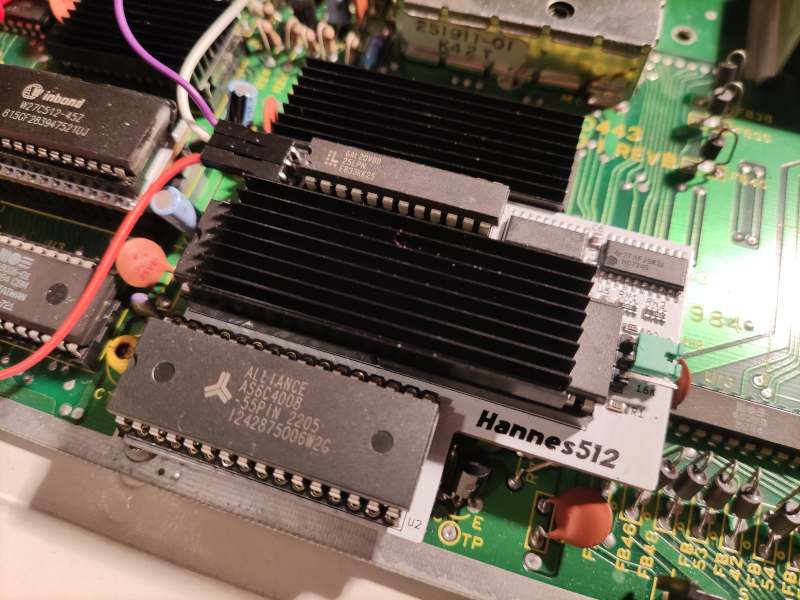
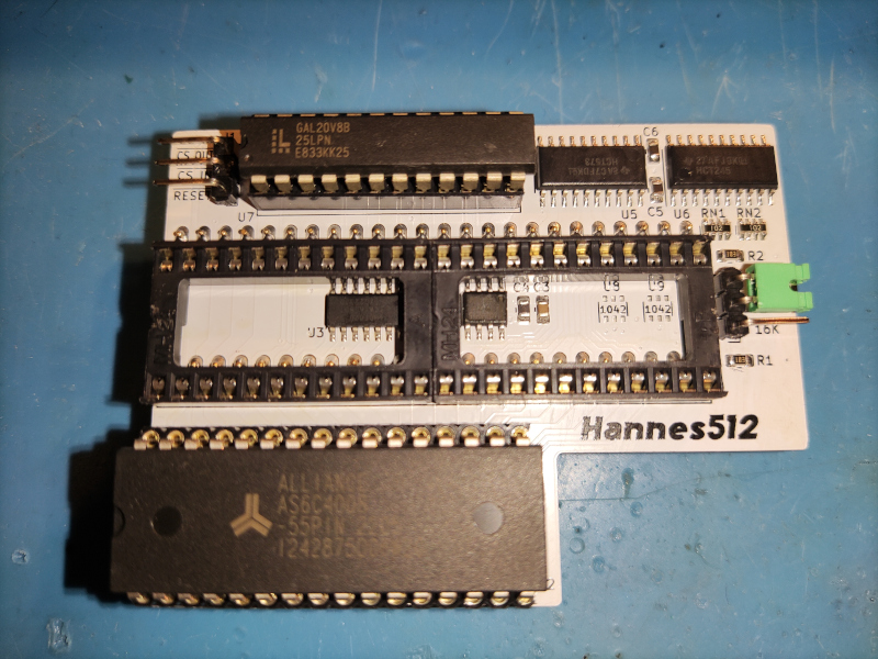
I made a V2 of the board, which included a full 8-bit register and a 74x245 allowing to read it back. Somehow I managed to squeeze it all in a single PCB (whose chip count grew to 15!), which was *almost* perfect: the 6529 replacement circuit was the one suggested by @TLC but I decided to use a NE555 instead of the 74x74 and that required the trigger signal to be inverted, which I overlooked. The fix was easy but then I didn't order the new PCBs immediately as I had a few more ideas to develop. That took its time and I placed the order right this week. Production is almost complete, I think the boards will be shipped tomorrow and there will be a lot to test then! I will change job, city and even country in about a month, so I really hope to manage to build and test everything before that, as settling down in the new context will definitely take some time and I won't be able to work on these things for a while.
On a side note, now I know the board fits inside the case nicely and it can be closed. I didn't measure the power consumption as I was sure it would have scared me! It seemed to work fine with the stock regulator anyway, but I didn't have anything else plugged in. Then I replaced the regulator with a 2A switching one just in case, and I think this board will just be one more reason to do that.
Hope to send another update soon .
|
|
Posted By
siz
on 2023-03-19
10:44:24
| Re: New Project: Hannes-compatible 256k RAM Expansion
As far as I recall (I don't remember where from): actually Csory expansion is activated when bit 4 and 5 are _different_ . It doesn't matter which one is 1 and which one is 0 as long as they are different. I'm not sure it was one of the PCX files in Solder's schematics ZIP or in the handwritten notes I got from Csory.
edit: just checked: you can see on 05.PCX that Csory expansion is activated by bit 4 and 5 connected to an XOR gate. So yes, the difference is that matters.
|
|
Posted By
TLC
on 2023-03-19
15:11:55
| Re: New Project: Hannes-compatible 256k RAM Expansion
@siz well, the PLD (which, I think we can agree that that should be the latest / definitive version) doesn't appear to support that.
Let me quote an excerpt from the 256KB_3.PLD file that describes the combinatorial logic in the GAL20V8.
MUX = A14* Q6* A15* Q7*/P5* P4* P6
+/A14*/Q6* A15* Q7*/P5* P4* P6
+ (....)
+/A14*/Q6*/A15*/Q7*/P5* P4*/P6*AEC
The GAL's MUX output controls, whether and when the page address from $FD15 bit0-3 (--> Q0-Q3 in Solder's schematics), is supposed to override the standard A14-A15 bits supplied by the mainboard, and the A16-A17 bits supplied by the base Hannes/Solder expansion logic. (06.PCX)
As you can see, every products have /P5 and P4 in them. From that on, it's beyond question that MUX can only ever be 1 (i.e. the Csory bank address can only take over, see 06.PCX) on the condition that P4=1 and /P5=1 - that is, P5=0.
So, P4=1, P5=0 is supposed to work, but P4=0, P5=1 isn't.
|
|
Posted By
siz
on 2023-03-19
15:34:37
| Re: New Project: Hannes-compatible 256k RAM Expansion
@TLC: I tend to disagree. A bit. Perhaps the intention was to work as You wrote and the discrete logic gate count was reduced to check the difference only. Or perhaps Solder ran out of GAL space so he tried to simplify the equations. But the original Hannes+Csory expansion is the discrete logic one. The GAL version should be backward compatible with that.
Tomorrow I'll try to dig up the handdrawn schematics given to me by Csory himself.
|
|
Posted By
TLC
on 2023-03-21
08:19:27
| Re: New Project: Hannes-compatible 256k RAM Expansion
@siz for me, things turn out like this,
- Code known to have been written by Csory himself ultimately always use P4=1, P5=0. (masm 256k too).
- Solder's ramregs.txt already does outline the "1 out of 4" schema for expansion logic activation. He got the particular bit combination documented wrong (...I think people are generally prone to overlook this whichever-similarly-looking-one-out-of-2 sort of choice in practice, I know I am), still, this clearly documents one thing, that is, a step made further from the "2 out of 4" (XOR gate based) activation schema. Thinking of Solder's, I certainly wouldn't have dared to invent this non-transparent modification by myself, without having reached an agreement with Csory over the matter first. (And AFAIK they're indeed known to have been sharing ideas and informations. Solder practically always detailed and documented the work previously done by Csory, Solder's SID-card has been voluntarily made compatible to Csory's, etc. etc. etc.) So I think even if, let's say, the idea of the final activation schema came from Solder rather than Csory, that definitely must have happened with Csory's knowledge and consent.
- Amongst the 256K capable setups assembled by Solder, should be at least a lot, that implement the P4=1, P5=0 activation schema. 256KB_3.PLD clearly shows that he has been actively using this, and he likely used the GAL based approach whenever possible, because, as he wrote, he specifically implemented that to reduce the amount of manual work necessary. (Agreed... by the existing Csory compatible setups once assembled by Solder, today, we're probably talking about a very small number.)
Christian probably still knows the definitive answer...
|
|
Posted By
SukkoPera
on 2023-03-29
06:28:42
| Re: New Project: Hannes-compatible 256k RAM Expansion
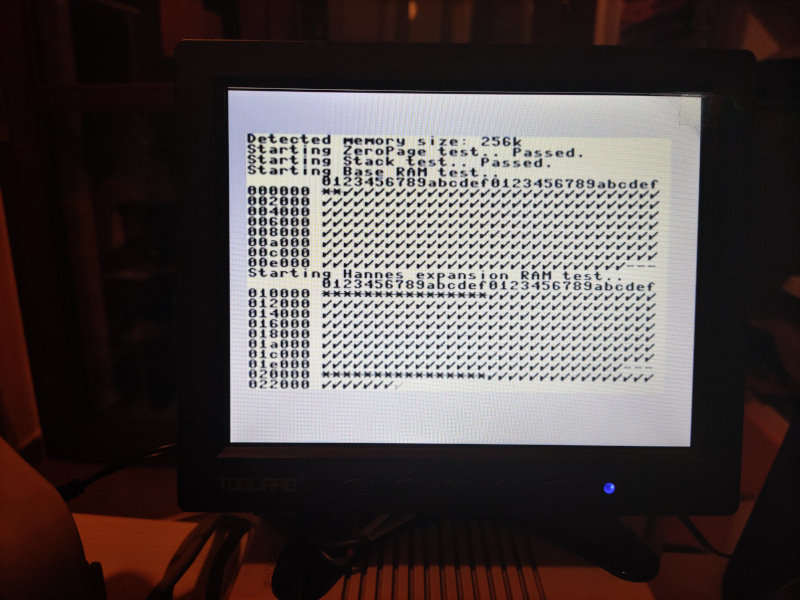
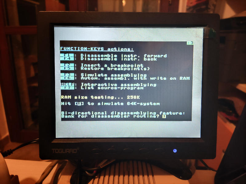
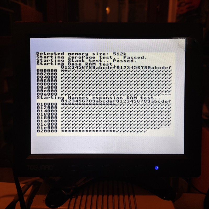
The V3 PCB has finally arrived and fully passed all tests so far! Siz's RAM test detects it successfully and reports no errors, and MegaAssembler detects it, too. I will test some more demos ASAP.
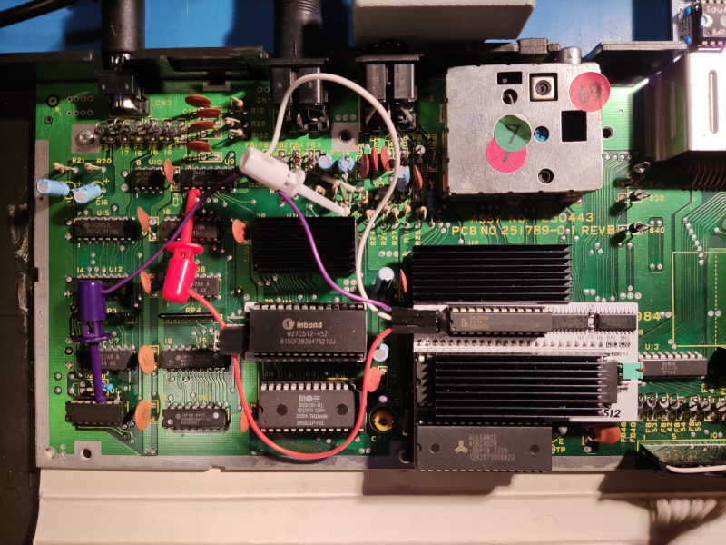
The case can be closed without any issues and the installation can be performed in a solderless fashion, if desired. Power consumption is still a mystery and will probably stay like that forever ;).
A switch is available in order to go back to the stock 16 kB configuration, but if that is not needed the 74LS257 multiplexers and the original RAM chips can be desoldered from the mainboard in order to save some power.

|
|
Posted By
siz
on 2023-03-29
09:24:59
| Re: New Project: Hannes-compatible 256k RAM Expansion
IMHO a single SRAM would have been a better choice because it occupies less space and consumes less power.
But the PCB looks very neat as usual. Congrats.
|
|
Posted By
SukkoPera
on 2023-03-29
14:50:31
| Re: New Project: Hannes-compatible 256k RAM Expansion
Your desire is my command, Sir .
|
|
Posted By
TLC
on 2023-03-30
04:35:55
| Re: New Project: Hannes-compatible 256k RAM Expansion
@SukkoPera: Wooooww!  
|
|
Posted By
SukkoPera
on 2023-03-30
05:33:38
| Re: New Project: Hannes-compatible 256k RAM Expansion
Hehehe, this one needs more testing, I literally assembled it the other night and was surprised it seemed to work first time!
I could have never made it without the other one though, it was a necessary step in understanding how the whole mechanism works. Actually it all started from a pretty straightforward 64k board I've never shown. You know, you make one step at a time .
Both the 256k and 512k boards have credits for you, @TLC, as the 6529 replacement circuit is basically the one you suggested. The 512k one also credits @eslapion, who explained to me how to get the SRAM working. You see how far we can get with open projects and collaboration? :)
By the way, apparently Dream World doesn't work with more than 256k. I thought it was a bug in my expansion but it behaves exactly the same on VICE configured for 1M (a 512k option is not available): it detects the RAM on the initial screen, then clears it and hangs on the grey background.
|
|
Posted By
siz
on 2023-03-30
09:18:15
| Re: New Project: Hannes-compatible 256k RAM Expansion
Nice work. Again!
I'll check (try to find time to check) Dream World on my 6502plus4 which also has 512k RAM.
A question: do your expansions use real 7501/8501 or a 6502 and emulate the CPU port too? (just hinting for next projects )
I really like that about the 6502plus4 (which is I think made by Eslapion) that I can save a plus/4 by replacing a dead 8501 with it.
|
|
Posted By
SukkoPera
on 2023-03-30
10:32:57
| Re: New Project: Hannes-compatible 256k RAM Expansion
These expansions get sandwiched between the TED and its socket, you can use any CPU (or replacement) you like...
... Provided that it physically fits! Maybe it's not clear from the pictures but my boards barely clear the CPU, any replacements that protrude towards the TED won't fit. This unfortunately rules out @MCes's excellent replacement . You can stack a few sockets to get around that but it might make the connections a bit unreliable.
|
|
Posted By
siz
on 2023-04-01
09:02:11
| Re: New Project: Hannes-compatible 256k RAM Expansion
Yeah, I was not aware that this goes under the TED (my 6502plus4 is a CPU replacement).
Today I had a little time to check Dream World. Yes, it really fails on machines with more than 256k RAM. The problem is that the power-up value of the RAM bank controller ($fd16) is $ff and for 256k RAM only the lower two bits are used but for 512k it's 3 bits.
This demo doesn't follow the rule that unused bits should be kept at their default values for future compatibility and changes bit 2 of the register (A18) from 1 to 0 - resulting in a crash. I've patched the loader to try it out but the 1541 loader also seems to be broken and I didn't have the patience to dig out a 1551 and real floppy disks to try that.
By putting a breakpoint in YaPE to catch $fd16 writes shows that this demo really uses the 256k expansion.
A quick workaround that came to my mind:
from BASIC:
MONITOR
>fd16 80
gfff6
And then load the demo. That way the RAM address bits will be initialized as the demo assumes. But that one fails too so there must be some other values it uses to write $fd16.
The conclusion is: the demo needs to be patched to work on machines with more than 256k memory. And on a 1541. :/
|
|
Posted By
SukkoPera
on 2023-04-07
18:30:41
| Re: New Project: Hannes-compatible 256k RAM Expansion
Thanks for your effort @siz, but unfortunately that doesn't make much of a difference, the demo still hangs in the same way.
Apparently, Lykia doesn't work correctly with 512 kB either: The second intro screen (the one with the "Plus/4" letters shifting into place) is a mess of colored squares, then the rest of the intro is OK but when the New/Continue game screen appears, it only has a white outline of what should be.
Again, I thought this was a fault of my expansion, but I "reduced" it to 256 kB by forcing bit 2 at $FD16 always high and both Dream World and Lykia work fine, which means the SRAM handling and the Hannes logic should be working correctly.
Am I right in thinking that with 512 kB the "default" page, i.e.: the one selected at startup and the one that is accessed when AEC and P6 are both low is bank 7 rather than bank 3? All bits being high by default should imply that. Does that make sense?
|
|
Posted By
siz
on 2023-04-08
05:40:46
| Re: New Project: Hannes-compatible 256k RAM Expansion
I'm not sure. I've betatested Lykia for Mad on my plus/4 with 6502 plus 4 (which also has 512k SRAM) and I've never had problems with it. But I'm not sure how the banking logic is implemented in 6502plus4.
Currently I am at the Revision party but I'll make some tests next week. What I know is that the initial value for $fd16 is $ff and Dream World does not work with my expansion while Lykia does. So yeah, I'll have to check.
|
|
Posted By
SukkoPera
on 2023-04-08
05:15:45
| Re: New Project: Hannes-compatible 256k RAM Expansion
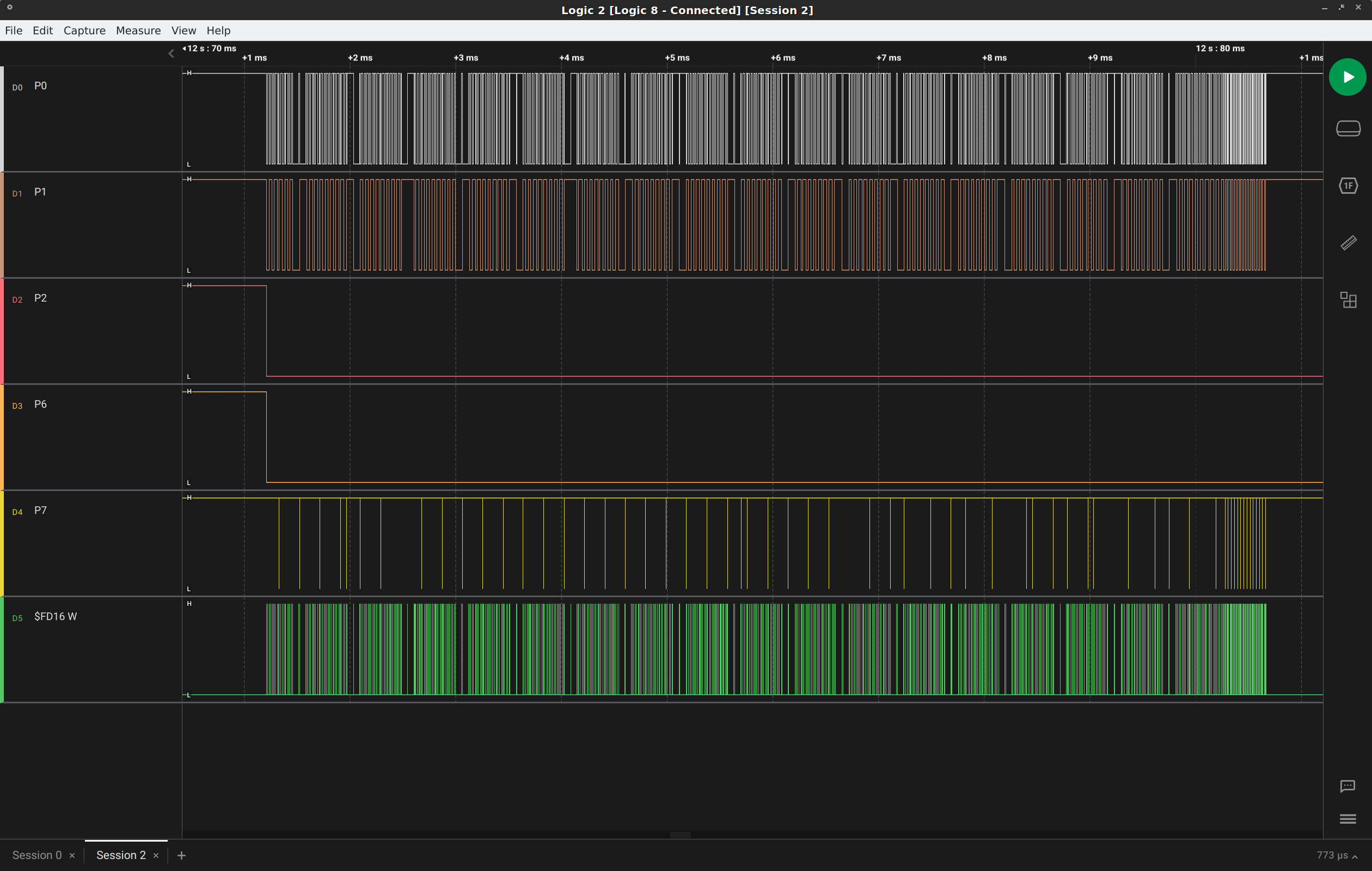
I had a look at what's going behind the scenes:
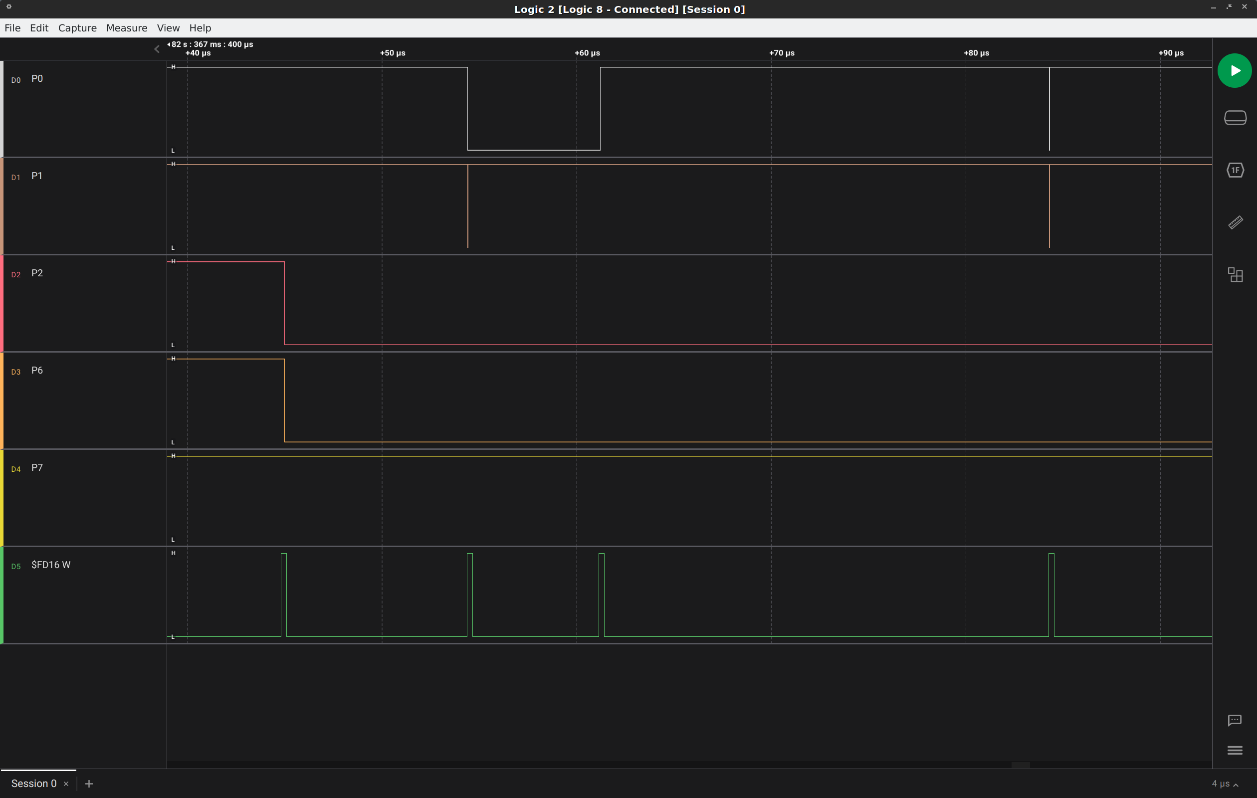
This is all that happens on $FD16 since the game starts up and until the New/Continue Game screen shows up. It shows about 50 us, all happenining at the game startup. My interpretation:
- All lines correctly start high.
- At startup the game plays a bit with the $FD16 contents, probably in order to see if extra memory is present.
- Then it settles to P6 = low (=> TED uses a fixed bank), P2 = low, P1 = P0 = high (=> Bank 3).
Now, I think I see what's going on, it's basically a matter of intepretation of Solder's original notes for P6:
Bit 6 1: Allowes TED-access to RAM (for text, graphic) to RAM-bank selected
with bits 0 and 1
0: TED-acces to RAM only in bank 3, bits 0 and 1 ignored
I had assumed that Solder was speaking of bank 3 because he only considered 256 kB (which implies 4 banks total), and that with more memory, his words should be intended as "the last bank", which is bank 7 when you have 512 kB (8 banks total).
And this is what I did in my implementation. What is happening is that my expansion is having TED always access bank 7 since P6 is low, but graphics data have probably been put in bank 3 by the CPU, since P2 is low.
The fix is easy (I would do it right now but I don't have my CUPL compiler at the moment) but the question is: is it correct that TED always accesses bank 3, rather than the last bank, when P6 is low?
The same question applies to accesses below $1000 (or below $4000 if P7 is low): Solder says:
The standard bank is bank 3.
The bank 3 is always in the nonswitchable area.
Should these always be directed at bank 3 or at the last bank, whichever it is?
@siz: Enjoy the party, no hurry :).
EDIT:
Here's what Dreamworld does, instead. Interestingly it does no writes to $FD16 for detection of the extra RAM. This all happens right before it crashes (but after it says it has detected 256 kB):
|
|
Posted By
siz
on 2023-04-08
05:45:30
| Re: New Project: Hannes-compatible 256k RAM Expansion
And this is what I did in my implementation. What is happening is that my expansion is having TED always access bank 7 since P6 is low, but graphics data have probably been put in bank 3 by the CPU, since P2 is low.
That's how I interpret it too.
About Dream World: as I remember it checks for the presence of the $fd16 register (it writes a value to $fd10 then compares it to $fd16). If that's successful (the values are different - it repeats the test with a different value if they are not) it just assumes that you have 256k.
|
|
Posted By
MCes
on 2023-04-08
09:31:28
| Re: New Project: Hannes-compatible 256k RAM Expansion
Hi, maybe it helps, maybe not....
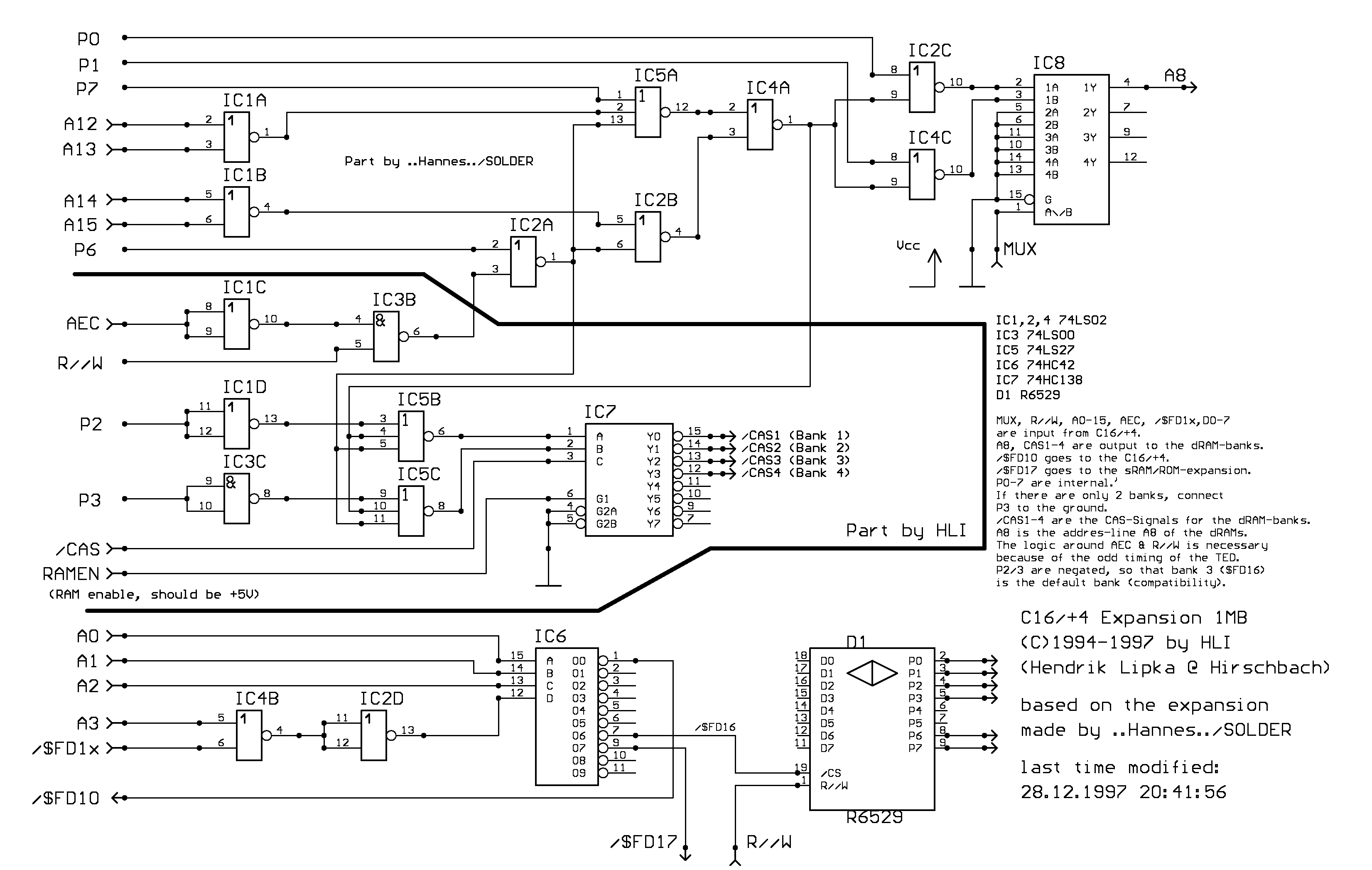
http://www.zimmers.net/anonftp/pub/cbm/documents/projects/memory/plus4/c16-to-1MB.gif
for more than 256k size (1M) I can read:
"P2/3 [MOS6529B outputs] are negated, so that bank3 ($FD16) is the default bank (compatibility)."
regardless of how many memory banks are implemented, the reference one always remains the number "3", for TED but also at startup for the CPU.
|
|
Posted By
siz
on 2023-04-08
16:53:03
| Re: New Project: Hannes-compatible 256k RAM Expansion
IMHO P2/P3 beeing inverted should not cause a problem as long as the register default value is $ff. This one should cause a problem only for TED reading the default bank.
But in case of Dream World the demo starts up in the highest memory bank (according to the control register at $fd16 as it's $ff by default) which is 7 for 512k then writes 3 to select bank 3. It does not care about inverting physical lines.
|
|
Posted By
MCes
on 2023-04-11
06:31:26
| Re: New Project: Hannes-compatible 256k RAM Expansion
I think that at the base of this kind of bug is a short-sighted (not lungimirante) chosen about the definition of TED access that is always limited at 256k and the highest bank is "3".
------------------------------------------------------------------------------------------------------
ramregs.TXT:
The control-register for the expansion is
located at adress $fd16 or 64790.
Bit 0/1 Select RAM-bank (0-3), standard is RAM-bank 3
Bit 4/5 Bit 5 4
            0 0: Activate expansion by Hannes
            0 1: Activate expansion by Hannes
            1 1: Activate expansion by Hannes
            1 0: Activate expansion by CSORY
Note: If you have no CSORY-expansion then set these bits both to "1"
or "0" for compatibility to CSORY-expansion.
This function is available also in CSORY-expansion-mode
Bit 7 Switch-bound:
0: >$0fff
1: >$3fff
Note: After switch-on the plus/4 all bits are "1". The standard bank is bank 3.
The bank 3 is always in the nonswitchable area.
-------------------------------------------------------------------------------------------------------
++++++++++++++++++++++++++++++
It was better if:
Bit 0/3 Select RAM-bank ($0-F), standard is RAM-bank $F:
it remain 256k/512k/1M compatible
(in case of <1M the extra bit/s has to remain not decoded and the expansion will be mirrored)
(...)
Bit 6 1: Allowes TED-access to RAM (for text, graphic) to RAM-bank selected
with bits 0,1,2,3
0: TED-acces to RAM only in bank $F, bits 0,1,2,3 ignored
Note: After switch-on the plus/4 all bits are "1". The standard bank is bank $F.
The bank $F is always in the nonswitchable area.
+++++++++++++++++++++++++++++++
remember:
bank=$F is "$F" into a 1M space, but it's a mirror of "7" into a 512k space, a mirror of "3" into a 256k space, so the "extended definition" of "default bank = $F" is always compatible.
The lack of the provision of being able to extend to more than 4 banks creates the possible SW/HW incompatibility,
but if the SW complies the the "extended definition" then it will be compatible with all 256k/512k/1M expansions.
did I get it right?
|
|
Posted By
SukkoPera
on 2023-04-11
06:36:09
| Re: New Project: Hannes-compatible 256k RAM Expansion
I have been thinking about the issue too, and you are perfectly right, @MCes. If the default bank had been specified as bank 15, we would not have this problem and everything would have worked the same with the 256kB expansion. It would have been a clean and future-prone solution.
BUT, I think, there is NOT YET any program that requires more than 256 kB and not much hardware that provides it, so we are still in time to define a behavior that works for us and maintains backwards compatibility with existing software and emulator implementations (which I have tried to analyze without much luck).
I don't think that simply inverting P2 is a smart choice: It's true that it will select bank 3 at startup, but that way when the program writes $x3 to $FD16, it will select bank 7.
With the way I implemented the 6529 replacement, the default value is provided by pull-up resistors. Therefore it should be sufficient to change those for P2 and P3 to pull-downs and I will have bank 3 selected at startup. Then I will change the GAL logic so that accesses to non-banked regions and TED accesses while P6=0 always get directed to bank 3. This way, bank 3 will maintain its "special status" even with expansions > 256 kB.
I think it would also be a good idea if programs didn't assume anything at startup and always explicitly selected the first bank they want to access. Most should be already doing so, luckily.
PS: "not lungimirante" = short-sighted :)
|
|
Posted By
MCes
on 2023-04-11
06:42:57
| Re: New Project: Hannes-compatible 256k RAM Expansion
@SukkoPera
Thanks for correct an error in translation of mine....
Another kind of solution is to make access at 3TH dimension:
the basic implementation remain 256k ($FD16 as usual),
but into $FD18 can be placed the extra bits for specify (CPU/TED) which of standard 256k blocks has to be addressed inside an area of 512k/1M/2M/....
Best compatibility also for future bigger expansion....
|
|
Posted By
siz
on 2023-04-11
17:22:29
| Re: New Project: Hannes-compatible 256k RAM Expansion
I'm just a programmer but please don't do new, incompatible extensions. (Even when there are very few actual programs that use 256k and even less computers having original 256k - or more - RAM expansions). The original Hannes expansion used a 6529 with initial value of $ff. Please keep it that way.
I can accept that address bits 18 and 19 in the bank select register (P2 and P3) are inverted and actually they select bank 3 as default (1111 xor 1100 in assembly ) and TED either accesses the same bank as the CPU or always bank 3.
I still don't understand why did they need this from a programmers point of view: the default bank is $0f (with whatever amount of RAM I have). When I set bit 6 to 0 TED will access only one of the banks. From a programmer's perspective it should be the default, power-up bank. And that's exactly what happens in the 1M expansion by HLI: internally he implements the default bank to be bank 3 (by inverting the upper two bank select bits of $fd16) and forces TED to read bank 3. But actually he would get the same result if he does not invert does bank select bits and just forces TED to bank $f.
It does not make sense to me to say that default bank is $f (the initial value of $fd16) and if you turn bit 6 of $fd16 to 0 to force TED to use a single bank it will be bank 3. And I know that this is what's written in the docs ("TED-acces to RAM only in bank 3, bits 0 and 1 ignored") but for them that was the default, the highest bank. And IMHO if we have more than 256k it should mean "bank select bits are ignored, default bank is used")
Returning to the bug in Dream World: as long as a program writes different bank select values and assumes them to have the same effect it will not work properly. Independently of hardware level tricks.
|
|
Posted By
SukkoPera
on 2023-04-12
04:56:29
| Re: New Project: Hannes-compatible 256k RAM Expansion
I agree that we shall not introduce any new mechanisms, but only do the bare minimum to understand how expansions > 256kB shall behave and make my own work this way.
I am not a +4 programmer, that's why I'm asking your help, @siz, in order to understand what I shall do, because this thing is going to be tricky and I see a lot of potential for incompatibilities, which can actually be already present in the few different implementations that are available.
So I will ask you a few questions, you should reply thinking purely as a programmer, please don't think about the hardware at all. Let's start with the following:
- Suppose you have switched to bank 1 to do some calculations on the data there. Now you need to switch back to the TED bank (assume P6=0) to make some data available to it: what value would you write to $FD16?
- Would you write a different value according to how much expansion memory is installed in the machine? Say 256kB, 512kB and 1 MB (suppose you have already found that out).
- What value to you expect to see from PRINT PEEK 64790 on a machine with a Hannes-style expansion and what value to you actually get on your 6502plus4-equipped machine? Please make a real test .
Thanks in advance!
|
|
Posted By
siz
on 2023-04-12
08:39:35
| Re: New Project: Hannes-compatible 256k RAM Expansion
- Suppose you have switched to bank 1 to do some calculations on the data there. Now you need to switch back to the TED bank (assume P6=0) to make some data available to it: what value would you write to $FD16?
It depends. In the nineties I would probably written
lda #$03 ; assuming I want bit 6&7 to be 0
sta $fd16
But then I also would have wrote
lda #$18
sta $ff07
to switch on multicolor mode, not caring about NTSC compatiblity
Nowadays (knowing that bit 2-3 can be address too) I would write
lda $fd16
and #$f0
ora #$0f
sta $fd16
or directly
lda #$3f ; assuming I want bit 6&7 to be 0
sta $fd16
- Would you write a different value according to how much expansion memory is installed in the machine? Say 256kB, 512kB and 1 MB (suppose you have already found that out).
No. I would like to use the power up value ($ff) as the default one.
- What value to you expect to see from PRINT PEEK 64790 on a machine with a Hannes-style expansion and what value to you actually get on your 6502plus4-equipped machine? Please make a real test happy.
I had to put your number into calculator to convert it to hexadecimal.
I expect it to be $ff (that register is documented to be a 6529 which powers up with $ff)
Let's see the test:

|
|
Posted By
MCes
on 2023-04-16
06:32:18
| Re: New Project: Hannes-compatible 256k RAM Expansion
If I understood well a clever SW use of $FD16 always make the SW wrote for 256K also compatible with 512K/1M expansion
(default bank always $F [bank3] for TED and for CPU, have a look some post before)
so the HW developer had only to extend the bank bits from 0,1 to 0,1,2,3 and ask to SW developers to correct the old SW that doesn't work with the "extended $FD16".
But is possible to note that there is not (into the database of the forum) a SW that use more than 256K,
so for future SW>256k another way could be chose for maintains 100% backwards compatibility with the old 256k $FD16 definition:
---------------------------- OLD -----------------------------------
$FD16 BIT(5,4):
0) 00 Activate expansion Hannes (not default)
1) 01 UNDEFINED: Activate expansion (GAL HW: Hannes)/(old HW: CSORY)
2) 10 Activate expansion CSORY
3) 11 Activate expansion Hannes (power up default)
-------------------------------------------------------------------
The previous OLD definition can be updated to 2M as follows:
************ NEW ***************
$FD16 BIT(5,4):
0) 00 Activate expansion Hannes [with extended $FD16 to 512k/1M: bit0,1,2,3 are considered] 1th slice of 2M expansion
1) 01 like as "0) 00" but banks from 2th "1M" slice in case of 2M expansion (default slice for TED and CPU is the 1th)
2) 10 Activate expansion CSORY
3) 11 Activate 256k expansion Hannes (power up default) [with old definition of $FD16 for 256k: only bit0,1 are considered]
Safely switching from "power up 256k" to "512K/1Mslice":
the HW>256k must consider the unused banks bits as "1", so switching from 256k to 512k/1M the new default bank ($F) will be the same of the previous power up default (3): ($3 'OR' $C=$F)
Bit 6
"H": Allowes TED-access to RAM (for text, graphic) to RAM-bank selected with bits 0,1,2,3 (default $F) from the selected slice: 1th or 2th (default 1th)
"L": TED-acces to RAM only in bank $F 1th slice (bits 0,1,2,3 and slice: ignored)
************************************
synthetically:
bit(5,4)
0 Hannes extended to 512k/1M (1th slice), bank(0..F) from bit0,1,2,3
1 Hannes extended to 2M (2th slice), bank(0..F) from bit0,1,2,3
2 CSORY
3 Hannes 256k (default) bank(0..3) from bit0,1
What choice for the future HW >256k?
|
|
Posted By
SukkoPera
on 2023-12-31
09:11:26
| Re: New Project: Hannes-compatible 256k RAM Expansion
As a new year's present, I have finally released all my memory expansions:
- Fixteen (64 kB)
- Hannes256 (256 kB)
- Hannes512 (512 kB)
Note that the 512 kB expansion is still subject to compatibility issues, so my suggestion is to limit it to 256 kB (can be done with a different GAL file which is provided) until we all manage to agree on how to properly handle the issue above. It is a mystery how the 6502plus4 works, as the problem is conceptual and cannot really be solved without patching at least some software.
|
|
Posted By
TLC
on 2024-04-05
03:21:57
| Re: New Project: Hannes-compatible 256k RAM Expansion
Following up on this old topic...
At the time I left there was a bit of a debate around how a prospective Csory expansion, and related expansion specific code was supposed to work (based on old documents plus anecdotal evidence).
In the meantime, I got reply from Christian. He confirmed that
- first versions of Csory's expansion schema used an XOR gate to activate the specific banking logic. That is, P4=0 / P5=1, and P4=1 / P5=0 both worked
- the revised (GAL based) design was introduced to reduce the work required to build memory expanded machines. This design omitted one of those combinations due to gate constraints, and from that on only the P4=1, P5=0 combination was kept
- for best compatibility with existing setups, the P4=1, P5=0 combination is supposed to be used
- this also implicitly confirms that this part in ramregs.txt:
Bit 4/5 Bit 5 4
0 0: Activate expansion by Hannes
0 1: Activate expansion by Hannes
1 1: Activate expansion by Hannes
1 0: Activate expansion by CSORY
is / has been wrong, in that either the header, or the list of combinations, have been mixed up.
That's all about that.
Re: 256k+ expansion schemas- and related page orders: I didn't follow that discussion since I haven't built (or even planned to build) such memory expansion myself yet. I still felt a bit of itching about that (that one seemed to be an issue with long term consequences right?...), and wanted to (and now in fact did) ask Christian about that as well, I just haven't received a reply to that question yet. However... to know beforehand what I were to talk about, I definitely had to chew on the subject a bit first, and I think I have some conclusions even right now. Let me just share them.
As we all know, the only legacy 256k+ logic schema is that of Hendrik Lipka's. This design still used multiple banks of 41256 dram chips (as the best available option at the time). Let me informally call HLI's design a bit "desperate", I mean even fitting the chips in the Plus/4's housing, and supplying power to the ram banks (we're talking about 32 dram chips for a 1M, and 16 for an 512k setup) had to be a considerably challenging task. I don't know how many machines have ever been expanded to 512k+ using that logic schema, let me make a guess that the result should be a very small number. I don't know about any legacy HLI 256k+ specific prods either.
This logic schema (as the root of this controversy I believe) has implemented extra logic to re-map the "default bank" to bank 3, by taking the following text from ramregs.txt literally.
Bit 6   1: Allowes TED-access to RAM (for text, graphic) to RAM-bank selected
           with bits 0 and 1
        0: TED-acces to RAM only in bank 3, bits 0 and 1 ignored
        This function is available also in CSORY-expansion-mode
Bit 7   Switch-bound:
        0: >$0fff
        1: >$3fff
Consequently, his schematics' notes literally say,
P2/3 are negated, so that bank 3 ($FD16) is the default bank (compatibility).
Now...
TL;DR: what had originally looked like a good idea to serve backwards compatibility, I think turned out to be a slight mistake, maybe something that creates a bit more confusion than benefit in practice. Let me just show that.
This is all really about what the "force default bank" mode of the Hannes / Solder schema is really doing in different setups. I think I'd better start explaining this one first, so that I could use it later on.
The "force default bank" condition is: whenever
- P6=1, P7=1, A14=A15=0, or
- P6=1, P7=0, A12=A13=A14=A15=0, or
- P6=0, AEC=0,
--> ignore bank selector bits, and revert to accessing the default bank (bank 3 in Hannes / Solder).
(See also, the quoted snippet above from ramregs.txt about Bits 6 and 7 of $FD16.)
If someone takes the time to study the schematics, they'll find out that, what the combinatorial logic is effectively doing, is this:
- P0 and P1 effectively controls (the multiplexed) A8 of the RAM banks (similarly to that of the predecessor Hannes logic)
- P2 and P3 controls, which 256k ram bank is selected (i.e. which 41256 dram bank receives /CAS).
...That is, "within-256k" and "which-256k" control is implemented (largely) separately.
- P0 and P1 are negated. That is, unless a "force default bank" condition happens, P0 and P1 control (mux) A8 in a negated fashion, i.e. P0=P1=0 implies A8=1 (the highest 64k physical page within a 256k memory bank).
- P2 and P3 are both negated twice, so P2=P3=0 selects /CAS1 (the lowest 256k memory bank), P2=1, P3=0 would fire /CAS2, and so on.
- If someone really checks what the "force default bank" condition logic induces, they'll find that it forces A8=0 and /CAS1 (the lowest 64k physical page within a 256k bank, and the lowest 256k bank, respectively).
Now after all that reverse engineering stuff, it would be high time to explain what this all really matters from a programmer's point of view, huh? So, to sum up what we effectively found:
- 64k banks within a 256k bank really work the same way to what would be expected from a stock Hannes / Solder expansion. A force-default condition selects the 64k bank that'd be selected by P0=P1=1, i.e. "bank 3", so this is perfect.
- 256k ram banks (out of four), from the other hand, work the opposite way. That is, force-default selects /CAS1 (lowest 256k bank), the 256k bank which is selected by P2=P3=0.
To sum up: this is literally consistent with what HLI has written in the notes, that is, the "default bank" is "bank 3", i.e. P0=1, P1=1, P2=0, P3=0. So far we have just proven what used to be already written in the docs, huh... Maybe a bit more actually, as the "force default" thing is probably not that simple at first sight (I know for me it wasn't), and that we cleared the detail that the "default bank" here is used in the meaning of "the bank to revert to", that is, upon force default bank conditions.
Why this all, after all, is a problem?
The short answer is: because this logic implicitly splits the "power on default" and "logic default" (so to call them) roles of the expansion register port bits, which'd matter after the machine had come out of power-on reset (...and anyway).
- Upon power-on reset, all bits in $FD16 are set to 1. This is inherent. $FD16 is a register implemented by a 6529B, it resets to "all bits=1" upon POR, it also reads as "all bits=1" at that point, there's nothing to do about it.
- In a Hannes / Solder expansion, both the "power-on" and the "logic" "default" banks mean the same, i.e. bank 3. (P0=1, P1=1). Any data written to RAM on an un-initialized Hannes / Solder machine ends just up written to bank 3.
- In the HLI expansion, however, the power on default bank is $0f (P0=1, P1=1, P2=1, P3=1), but the "logic" default (the page to revert to upon force-default conditions) is bank 3 (P0=1, P1=1, P2=0, P3=0). Now, given that someone powers up HLI's 1Meg machine, and given that the $FD16 power-on default sets up a force-default condition for the $0000-$3fff window (which it does), the following would happen. Anything written to RAM on the uninitialized machine, ends up written to bank 3 in the $0000-$3fff address range, and written to bank $0f in $4000-$ffff. This is a problem.
The scope of this problem includes data written by Kernal Reset, Basic Reset, and Kernal Load (just to name the most obvious/important ones), basically anything before some 256k specific code eventually hits, and initializes $FD16. Say, some particular stuff gets loaded by the Kernal Load, and then this code and data gets unpacked by some stock, non-256k aware embedded unpack code (...a very realistic scenario in practice) in the next step. In that case, all the stuff's bits and pieces below the $4000 mark end up depacked to bank 3, and above $4000, to bank $0f. Now imagine that the stuff now changes $FD16 Bit 7 (P7=0) to reduce the common page window to $0000-$0fff from the default $0000-$3fff range (also a pretty sensible move), and plays also nicely so it only changes the P7 control bit, leaving the rest of the $FD16 control bits alone. On stock Hannes / Solder, that move would be harmless, remember, both below and above the $4000 mark, there'd be bank 3. But on HLI's, that move maps in bank $0f for the $1000-$3fff range as well - which has no meaningful data yet... whoopsie... Also, let's suppose, some code uses force default bank mode for TED memory accesses (it sets P6=0) at some point, and has graphic data previously unpacked somewhere above the $4000 mark. Now this data is residing in bank $0f, and the force-default bank triggers TED graphic data fetch from bank 3... that wouldn't likely look that nice, would it... TL;DR: the HLI setup would at least additionally require the user to select bank 3 manually prior to attempting to load and run 256k specific stuffs in any case (to overcome the "power-on default != logic default" issue), for the thing to have the slightest chances to work properly.
(Also imagine some hypothetic ROM expansion that'd say O.K., I'll just "fix" this by setting bank 3 as part of the ROM Reset routine. Now, anything 256k+ specific stuff non-aware of that, would crash on data not residing in bank $0f after a stock Load as it'd expect. For sure there are endless possibilities to raise yet more confusion.)
I wouldn't deal with non-at-least-somewhat-behaving cases (i.e. stuff absolutely non working on a 256k+ setup), I mean people have been very obviously free to use bits P2 and P3 arbitrarily in their stuffs anyway, and as they have, there really isn't supposed to exist one single hypothetic works-for-all-cases 256k-backwards-compatible 256k+ solution anymore (except for the hw option to disconnect all the extra bank selector bits, of course - which'd, just to mention, would by itself rule out the HLI hack's value, given that the hw solution would effectively revert the expansion logic to behave like a true stock 256k Hannes / Solder thing all by itself). All in all, I see little improvement in the HLI default bank hack by means of anything that'd really enhance backwards compatibility, yet I see it something that makes the whole memory expansion thing a bit even more messy, a bit more ugly, if I may say. If someone asked me, at this point I'd seriously suggest refraining from dragging this on for any hypothetic "standard" 256k+ Hannes / Solder descendant expansion schemas, I'd just suggest keeping the basic linear formula to access banks above the 256k mark (--> both the "power-on" and "logic" default banks being defined as the "highest available 64k bank", that is, the bank selected by "all selector bits = 1"), and have any possibly bad-behaving legacy 256k specific code (...whose possible existence would be evident with- or without the HLI addition anyway) be patched for that setup.
|
|
Posted By
SukkoPera
on 2024-04-04
17:20:29
| Re: New Project: Hannes-compatible 256k RAM Expansion
@TLC: I'll read your post again tomorrow when I'm less tired, but I think you pointed out the same problem I have been talking about for a while: if P2/3 are negated, meaning that the power-up default of $0F actually points to block $03, this implies that when the program switches to a different block and then wants to switch back to the default block writing $03, it is actually switching to $0F, which is a different bank.
The way for the future is simple: just write $0F to switch to the default bank, regardless of the amount of memory installed, that will always work (well, actually you will need to handle the high nibble properly but you get the idea).
But the problem is that there is no 512 kB configuration that will work with ALL of the 256 kB software that currently exist, whatever trick you play will get some working but will break this or that. I really wonder how the 6502plus4 can manage to get everything working (if it actually is).
|
|
Posted By
TLC
on 2024-04-05
08:19:51
| Re: New Project: Hannes-compatible 256k RAM Expansion
@SukkoPera I think the basic confusion about this matter is in the context of this "default bank" thing, I mean how this "default" word is interpreted.
It's no matter how some address bits are inverted (negated) in some particular memory addressing schema. Such thing is nothing more than a logical mapping, which makes no difference as long as all the interested parties know about the exactly same one. (See, if I'd to invert A16 or A17 in some banking logic, application level wouldn't notice that, since it'd still see a linear N-bit address space. Whether some addresses now resided on different physical memory pages than before, it'd really not care.) Some problem can only pop up from the point where the physical memory can be addressed multiple ways. This is exactly the case with Hannes / Solder's "force-default bank" thing, where it's implicitly a second way to address physical memory banks. Still, the detail that "where exactly" some difference is actually happening in the combinatorial logic, doesn't really matter either, as far as the end result is concerned. The only thing that really matters, is just how the different addressing methods "relate" to each other.
In effect, and from a purely logical (not implementation) point of view, in HLI's you get
- a usual linear bank addressing schema from bank 0 to N (N=$0f for 1M), with the "highest existing" bank set active on power-on reset (...this schema totally aligning with that of original Hannes / Solder so far).
- "bank 3" of the linear bank address range selected on "force default bank" conditions
The latter, "bank 3" thing is implemented by manipulating the P2 and P3 signals. TL;DR: this detail doesn't really matter. (The author could as well have manipulated the "force default" combinatorial logic to achieve the same result... I mean this is a mere detail of physical implementation. What only matters is how the selected bank of the basic bank addressing method relates to the selected bank by the other (force-default-bank) method. This relation can be deduced by interpreting the combinatorial logic, i.e. finding out what MA8 and /CAS is triggered by a force-default-bank condition, and then finding out, which P0-P3 values trigger the same MA8 and /CAS values. That's where actually the force-default-bank = P0=1, P1=1, P2=0, P3=0 result comes from).
That's probably all about the HLI specific bank addressing schema.
Personally I think that "well behaving" 256k/256k+ specific code is and has always been supposed to leave unused bits of $FD16 just alone. I mean the one single guaranteed thing here is, that all bits in $FD16 are initialized to "1" upon power-on reset. Logically, and that's maybe only because I had read a lot of microcontroller / other embedded system related application notes in my life , that default would have to be respected for any bits not needed / not "known about" by the code (--> mask them and keep them "1" all time), and from that point on, things would-should just work fine on any Hannes / Solder derivatives of any size. (Note, that that simple rule is messed up by the HLI address hack for any 256k+ Hannes / Solder derivatives, if implemented.) That method would work for any Hannes / Solder / Csory combinations up to 1M, and for up to 4M pure Hannes / Solder derivatives (where P4 and P5 also play as bank address bits).
As said, considering that people could and likely have arbitrarily set the P2-P5 bits in their legacy 256k specific prods, from the point P2-P3(-P5) have effect, I think there's little chance that one-single 256k+ schema could fit all the existing cases in one. I guess this is an inherent limitation.
(I think, for bad-behaving 256k code, the best options are probably a revert-to-256k hw mode first - that is, a hw option (either activated by config bits or a physical switch), where bank select bits from P2 and above are void of any effect on memory addressing. That'd plausibly make all the affected legacy prods work "in one step", albeit with manual intervention needed. Patching problematic code as time goes (so that they would "behave"), could then make these prods run on "regular" expanded memory setups of any expansion sizes just out of the box,... that is, no longer requiring manual intervention.)
|
|
| |
Copyright © Plus/4 World Team, 2001-2025. Support Plus/4 World on Patreon |