Posted By

TLC
on 2024-04-05
03:21:57
|  Re: New Project: Hannes-compatible 256k RAM Expansion Re: New Project: Hannes-compatible 256k RAM Expansion
Following up on this old topic...
At the time I left there was a bit of a debate around how a prospective Csory expansion, and related expansion specific code was supposed to work (based on old documents plus anecdotal evidence).
In the meantime, I got reply from Christian. He confirmed that
- first versions of Csory's expansion schema used an XOR gate to activate the specific banking logic. That is, P4=0 / P5=1, and P4=1 / P5=0 both worked
- the revised (GAL based) design was introduced to reduce the work required to build memory expanded machines. This design omitted one of those combinations due to gate constraints, and from that on only the P4=1, P5=0 combination was kept
- for best compatibility with existing setups, the P4=1, P5=0 combination is supposed to be used
- this also implicitly confirms that this part in ramregs.txt:
Bit 4/5 Bit 5 4
            0 0: Activate expansion by Hannes
            0 1: Activate expansion by Hannes
            1 1: Activate expansion by Hannes
            1 0: Activate expansion by CSORY
is / has been wrong, in that either the header, or the list of combinations, have been mixed up.
That's all about that.
Re: 256k+ expansion schemas- and related page orders: I didn't follow that discussion since I haven't built (or even planned to build) such memory expansion myself yet. I still felt a bit of itching about that (that one seemed to be an issue with long term consequences right?...), and wanted to (and now in fact did) ask Christian about that as well, I just haven't received a reply to that question yet. However... to know beforehand what I were to talk about, I definitely had to chew on the subject a bit first, and I think I have some conclusions even right now. Let me just share them.
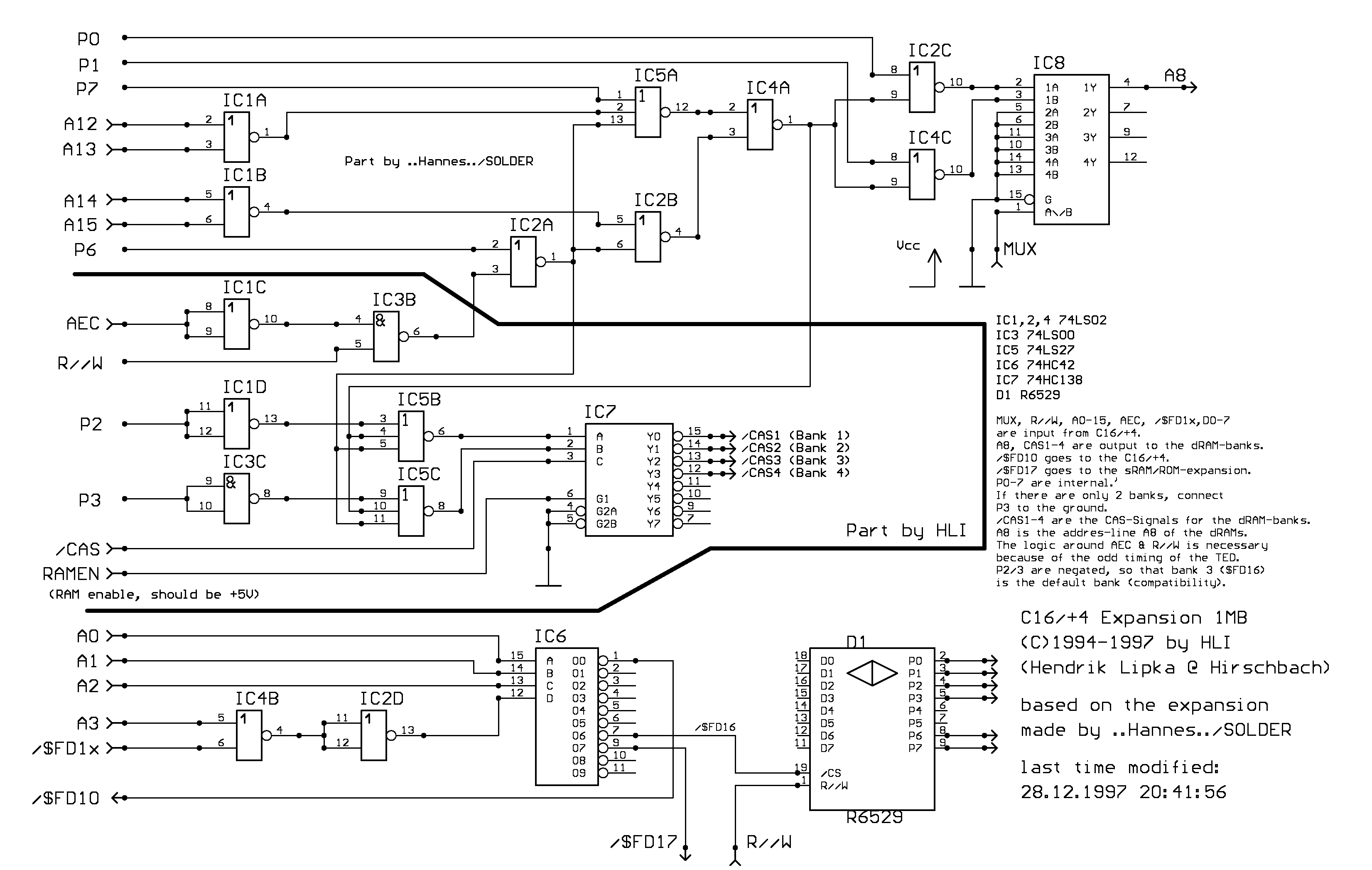
As we all know, the only legacy 256k+ logic schema is that of Hendrik Lipka's. This design still used multiple banks of 41256 dram chips (as the best available option at the time). Let me informally call HLI's design a bit "desperate", I mean even fitting the chips in the Plus/4's housing, and supplying power to the ram banks (we're talking about 32 dram chips for a 1M, and 16 for an 512k setup) had to be a considerably challenging task. I don't know how many machines have ever been expanded to 512k+ using that logic schema, let me make a guess that the result should be a very small number. I don't know about any legacy HLI 256k+ specific prods either.
This logic schema (as the root of this controversy I believe) has implemented extra logic to re-map the "default bank" to bank 3, by taking the following text from ramregs.txt literally.
Bit 6   1: Allowes TED-access to RAM (for text, graphic) to RAM-bank selected
           with bits 0 and 1
        0: TED-acces to RAM only in bank 3, bits 0 and 1 ignored
        This function is available also in CSORY-expansion-mode
Bit 7   Switch-bound:
        0: >$0fff
        1: >$3fff
Consequently, his schematics' notes literally say,
P2/3 are negated, so that bank 3 ($FD16) is the default bank (compatibility).
Now...
TL;DR: what had originally looked like a good idea to serve backwards compatibility, I think turned out to be a slight mistake, maybe something that creates a bit more confusion than benefit in practice. Let me just show that.
This is all really about what the "force default bank" mode of the Hannes / Solder schema is really doing in different setups. I think I'd better start explaining this one first, so that I could use it later on.
The "force default bank" condition is: whenever
- P6=1, P7=1, A14=A15=0, or
- P6=1, P7=0, A12=A13=A14=A15=0, or
- P6=0, AEC=0,
--> ignore bank selector bits, and revert to accessing the default bank (bank 3 in Hannes / Solder).
(See also, the quoted snippet above from ramregs.txt about Bits 6 and 7 of $FD16.)
If someone takes the time to study the schematics, they'll find out that, what the combinatorial logic is effectively doing, is this:
- P0 and P1 effectively controls (the multiplexed) A8 of the RAM banks (similarly to that of the predecessor Hannes logic)
- P2 and P3 controls, which 256k ram bank is selected (i.e. which 41256 dram bank receives /CAS).
...That is, "within-256k" and "which-256k" control is implemented (largely) separately.
- P0 and P1 are negated. That is, unless a "force default bank" condition happens, P0 and P1 control (mux) A8 in a negated fashion, i.e. P0=P1=0 implies A8=1 (the highest 64k physical page within a 256k memory bank).
- P2 and P3 are both negated twice, so P2=P3=0 selects /CAS1 (the lowest 256k memory bank), P2=1, P3=0 would fire /CAS2, and so on.
- If someone really checks what the "force default bank" condition logic induces, they'll find that it forces A8=0 and /CAS1 (the lowest 64k physical page within a 256k bank, and the lowest 256k bank, respectively).
Now after all that reverse engineering stuff, it would be high time to explain what this all really matters from a programmer's point of view, huh? So, to sum up what we effectively found:
- 64k banks within a 256k bank really work the same way to what would be expected from a stock Hannes / Solder expansion. A force-default condition selects the 64k bank that'd be selected by P0=P1=1, i.e. "bank 3", so this is perfect.
- 256k ram banks (out of four), from the other hand, work the opposite way. That is, force-default selects /CAS1 (lowest 256k bank), the 256k bank which is selected by P2=P3=0.
To sum up: this is literally consistent with what HLI has written in the notes, that is, the "default bank" is "bank 3", i.e. P0=1, P1=1, P2=0, P3=0. So far we have just proven what used to be already written in the docs, huh... Maybe a bit more actually, as the "force default" thing is probably not that simple at first sight (I know for me it wasn't), and that we cleared the detail that the "default bank" here is used in the meaning of "the bank to revert to", that is, upon force default bank conditions.
Why this all, after all, is a problem?
The short answer is: because this logic implicitly splits the "power on default" and "logic default" (so to call them) roles of the expansion register port bits, which'd matter after the machine had come out of power-on reset (...and anyway).
- Upon power-on reset, all bits in $FD16 are set to 1. This is inherent. $FD16 is a register implemented by a 6529B, it resets to "all bits=1" upon POR, it also reads as "all bits=1" at that point, there's nothing to do about it.
- In a Hannes / Solder expansion, both the "power-on" and the "logic" "default" banks mean the same, i.e. bank 3. (P0=1, P1=1). Any data written to RAM on an un-initialized Hannes / Solder machine ends just up written to bank 3.
- In the HLI expansion, however, the power on default bank is $0f (P0=1, P1=1, P2=1, P3=1), but the "logic" default (the page to revert to upon force-default conditions) is bank 3 (P0=1, P1=1, P2=0, P3=0). Now, given that someone powers up HLI's 1Meg machine, and given that the $FD16 power-on default sets up a force-default condition for the $0000-$3fff window (which it does), the following would happen. Anything written to RAM on the uninitialized machine, ends up written to bank 3 in the $0000-$3fff address range, and written to bank $0f in $4000-$ffff. This is a problem.
The scope of this problem includes data written by Kernal Reset, Basic Reset, and Kernal Load (just to name the most obvious/important ones), basically anything before some 256k specific code eventually hits, and initializes $FD16. Say, some particular stuff gets loaded by the Kernal Load, and then this code and data gets unpacked by some stock, non-256k aware embedded unpack code (...a very realistic scenario in practice) in the next step. In that case, all the stuff's bits and pieces below the $4000 mark end up depacked to bank 3, and above $4000, to bank $0f. Now imagine that the stuff now changes $FD16 Bit 7 (P7=0) to reduce the common page window to $0000-$0fff from the default $0000-$3fff range (also a pretty sensible move), and plays also nicely so it only changes the P7 control bit, leaving the rest of the $FD16 control bits alone. On stock Hannes / Solder, that move would be harmless, remember, both below and above the $4000 mark, there'd be bank 3. But on HLI's, that move maps in bank $0f for the $1000-$3fff range as well - which has no meaningful data yet... whoopsie... Also, let's suppose, some code uses force default bank mode for TED memory accesses (it sets P6=0) at some point, and has graphic data previously unpacked somewhere above the $4000 mark. Now this data is residing in bank $0f, and the force-default bank triggers TED graphic data fetch from bank 3... that wouldn't likely look that nice, would it... TL;DR: the HLI setup would at least additionally require the user to select bank 3 manually prior to attempting to load and run 256k specific stuffs in any case (to overcome the "power-on default != logic default" issue), for the thing to have the slightest chances to work properly.
(Also imagine some hypothetic ROM expansion that'd say O.K., I'll just "fix" this by setting bank 3 as part of the ROM Reset routine. Now, anything 256k+ specific stuff non-aware of that, would crash on data not residing in bank $0f after a stock Load as it'd expect. For sure there are endless possibilities to raise yet more confusion.)
I wouldn't deal with non-at-least-somewhat-behaving cases (i.e. stuff absolutely non working on a 256k+ setup), I mean people have been very obviously free to use bits P2 and P3 arbitrarily in their stuffs anyway, and as they have, there really isn't supposed to exist one single hypothetic works-for-all-cases 256k-backwards-compatible 256k+ solution anymore (except for the hw option to disconnect all the extra bank selector bits, of course - which'd, just to mention, would by itself rule out the HLI hack's value, given that the hw solution would effectively revert the expansion logic to behave like a true stock 256k Hannes / Solder thing all by itself). All in all, I see little improvement in the HLI default bank hack by means of anything that'd really enhance backwards compatibility, yet I see it something that makes the whole memory expansion thing a bit even more messy, a bit more ugly, if I may say. If someone asked me, at this point I'd seriously suggest refraining from dragging this on for any hypothetic "standard" 256k+ Hannes / Solder descendant expansion schemas, I'd just suggest keeping the basic linear formula to access banks above the 256k mark (--> both the "power-on" and "logic" default banks being defined as the "highest available 64k bank", that is, the bank selected by "all selector bits = 1"), and have any possibly bad-behaving legacy 256k specific code (...whose possible existence would be evident with- or without the HLI addition anyway) be patched for that setup.
|