| Posted By

SukkoPera
on 2022-10-27
17:43:43
|  Let's remake the DigiBlaster! Let's remake the DigiBlaster!
Now that we have replicated Solder's SIDcard, why not replicate the DigiBlaster, too?
Unfortunately Solder hasn't released the schematics for this board AFAIK, thus I really need your help! I don't have the actual board and I have already done the best I could, which is look closely at the available pictures and try to understand what components are used and how they are interconnected.
The problem is that this board is mostly analog stuff, which means I'm at a total loss. Besides a few obvious connections, I have no idea of how everything works together.
I have placed all the components in some KiCad schematics, assigned footprints and tried to lay them out similarly to how they are on the board. The full project is available on GitHub, here's how it currently looks (yeah, I know the shape is a bit different but that's ok at this time):
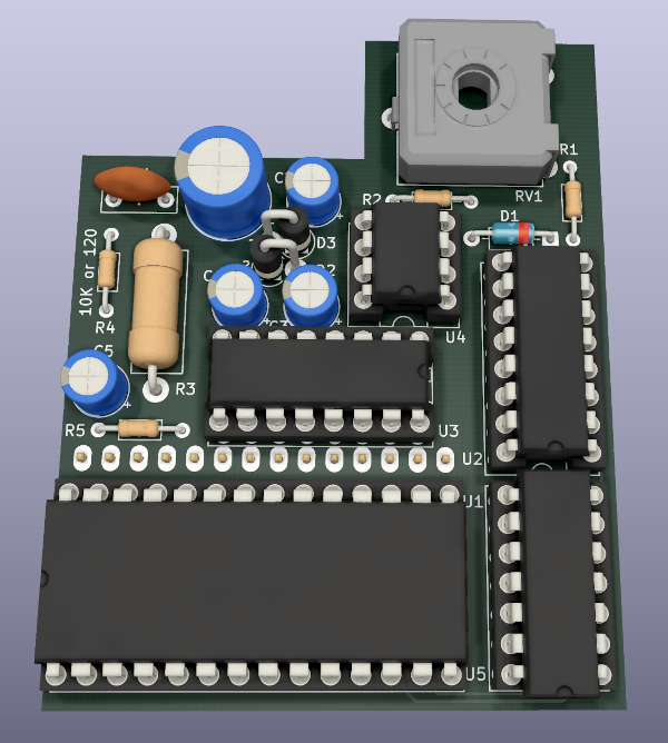
What I would need is that someone with an actual board, a decent multimeter, a pair of good eyes and 10 minutes of their time went over their board and checked that the type and values of all components in this other picture are correct when specified and filled them in when they aren't.
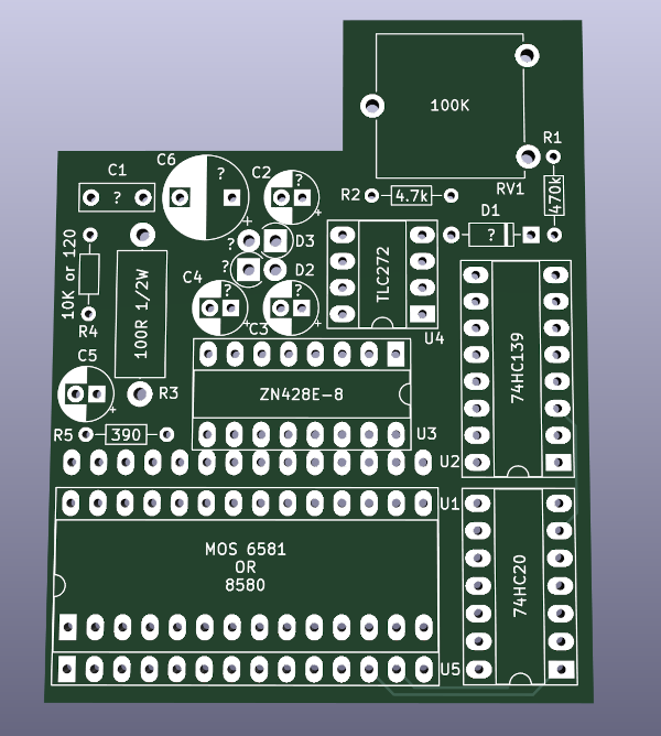
It would be great if this could be done directly in the Kicad project but even if you don't know how to do that, you can still help: I have already assigned names to all components so just post here saying, for instance: R4 = 10k, D1 = 1n4148, etc.
I would also love to get high-resolution pictures of the top (remove the SID and any other components you can) and bottom of the board, with all the traces visible.
The final step will be going over the board with a multimeter in continuity mode and trace all the tracks that cannot be seen clearly.
As usual, the whole project will be openly released under the CC-NC-BY-SA license.
Can you help? 
|
|
Posted By
TLC
on 2022-11-02
18:37:19
| Re: Let's remake the DigiBlaster!
Someone in possession of this card would really need to step in and give some help here IMHO. Let me explain.
I also only know photos of this card, no schematics, and no examples that I could have ever inspected closely. (While I could see maybe a dozen of Synergy SID card examples in the last 25+ years, I've seen no DigiBlasters, literally not a single example. Which makes it also very little risky to say, that the number of DigiBlaster examples ever produced, must be very small). For some time, I thought that the A/D part of this card must have worked in a partly software supported manner (that is - successive approximation code that'd use the D/A converter and one half of the TLC272 op-amp wired as a comparator) - since, the card seemingly employed no dedicated A/D converters.
...But I've just taken the digitizer code of Apos' Digital Composing Kit V2.0 apart, and found apparently no signs of any extra steps done there. Which leads to the conclusion that we probably don't even know every components yet, there has to be also an A/D converter there (a ZN427 or something like that, somewhere hidden) in the first place.
|
|
Posted By
MMS
on 2022-11-03
15:37:50
 | Re: Let's remake the DigiBlaster!
If you check the Digiblaster picture of Synergy you can see the Ferranti.
ZN428E is the Ferranti IC 8 bit wonder i also used for my great sounding Covox I made for my PC in 1995. Great stuff with trackers and pinball dreams. I suppose if is much easier to implement on user port 8 bit output than mapping to a certain register.
Sure, it would be without any support, not like the Digiblaster.
|
|
Posted By
gerliczer
on 2022-11-03
17:19:14
| Re: Let's remake the DigiBlaster!
It is probably safe to say that SukkoPera and TLC both know about that IC. Their problem is the apparent lack of anything suitable to do the A/D conversion DigiBlaster is said to feature. SID's ADC is slow and low resolution so it is improbable that it is being used.
|
|
Posted By
SukkoPera
on 2022-11-03
18:25:28
| Re: Let's remake the DigiBlaster!
Yeah, we all see the Ferranti (U3 in my board reproduction), but that would be the DAC. The Digiblaster is supposed to also have an ADC onboard (say a sampler), but it's definitely not visible in the pictures. It must either lie below the SID (my guess, just like the 74LS245 on the SIDcard) or ADC conversion must be done with one channel of the opamp (U4) a lot of help from software (TLC's hypothesis).
I have been trying to guess how address decoding is done (that's what the 74HC20 and 139 are there for) and I *think* that it's so convoluted because two Chip Select signals need to be generated, one for the DAC and one for the ADC. I think it could be done more simply if only the one for the DAC was needed but it's all speculation of course.
So the Digiblaster is a rare thing, I didn't expect that! There are quite a lot of people talking about it here and there plus it is emulated almost everywhere, which surprises me a bit if emulator coders never even had access to one!
Anyway, if that's the case, it's one more reason to make a replica! If anyone has one but doesn't feel like doing the job, I am also keen on taking care of everything if they ship it to me. I will also be glad to return it along with a few presents  . .
EDIT: Hey, look at this smaaaall pic from Solder's page, it's the only one I found of a Digiblaster without a SID plugged in:
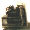
I know it's tiny but... Do you see what I see, right in the middle of the SID socket? ;)
|
|
Posted By
TLC
on 2022-11-04
06:18:07
| Re: Let's remake the DigiBlaster!
Good, at least that part of the mystery seems to be solved .
Emulation - well, from software, the DigiBlaster merely looks like a pair of registers, i.e. a 8 bit D/A register at base +$1E, and another 8-bit A/D register at base + $1F, respectively. (By base + $1E I mean both $FD5E and $FE9E etc., as usual in this card). IMHO it's quite trivial to emulate.
Address decoding - I think the decoding logic has to provide at least three CS' signals, i.e. +$1E_write, +$1F_read, and also +$1F_write. The reason for +$1F_write is that 1.) the digitizer code in the Digital Composing Kit very obviously writes the $FD5F address every once after it had read it, which aligns well with the fact that 2.) successive approximation A/D converters typically need a strobe to actually start the conversion process.
(Note also - the address decoder needs to exclude the DigiBlaster's assigned 2 addresses from the onboard SID's chip select.)
BTW, if I'd have to make a guess about the A/D, I'd probably say the ZN427. (Now thinking it over, that's gonna be a somewhat challenging quest... I mean not just technically but logistically... AFAIR poor Ferranti i.e. the producer of the ZN series has been out of business for the last 30 or so years now... forget it; did a bit of search, and, fortunately, Ferranti's semiconductor business appears to have survived (--> it became Zetex) ).
|
|
Posted By
MMS
on 2022-11-04
05:26:55
| Re: Let's remake the DigiBlaster!
Aaaah, sorry... I was in hurry and read DAC and not ADC.
Original Ferranti ICs not only rare but rather expensive too.
But they produce much better sound quality that the resistance ladder for the same task.
I am sure there are some cheaper China copies too.
So it should be ZN427. I have seen only one piece in my lifetime, my roommate made a digitizer for his A500+, it was in 1994.
It was really small, the whole circuitry fit into the housing of a centronics connector., though he adjusted the signal level externally.
|
|
Posted By
gerliczer
on 2022-11-04
05:50:58
| Re: Let's remake the DigiBlaster!
Nice catch, SukkoPera.  Unfortunately, that could be anything. Unfortunately, that could be anything.  I did a cursory search on ZN427s. It gave one place where you could seemingly order such an IC at around 18 EUR per piece. But here's a question. Do you want to build an exact replica or a functionally equivalent device? The first may prove impossible without access to an original board. The last has less old school glamour. I did a cursory search on ZN427s. It gave one place where you could seemingly order such an IC at around 18 EUR per piece. But here's a question. Do you want to build an exact replica or a functionally equivalent device? The first may prove impossible without access to an original board. The last has less old school glamour.
|
|
Posted By
SukkoPera
on 2022-11-05
08:26:50
| Re: Let's remake the DigiBlaster!
@TLC: The SIDcard address decoder cannot exclude $FD5E/F from the SID range because it does not get A3/2/1, but luckily the SID doesn't respond to the last three addresses so I guess it won't drive the bus even if selected. That must be why Solder chose those addresses. I think the address decoding on the Digiblaster just uses the SID /CS plus a4...a0 to produce all the signals it requires.
The ZN428E can be found easily and cheaply on AliExpress & such. They're definitely second hand pulls but usually a good part of those works fine. Unfortunately the 427 is much harder to find, I think I only found the same one mentioned by @MMS, there are no signs of it on Chinese portals .
@gerliczer: Well, both . I usually start with a 1:1 replica, both for documentation purposes and to have a solid starting point for subsequent modifications and evolution, so I really hope someone here has at least one board we can analyze. As for a practical realization, I'm more concerned in the board having at least the DAC. I'm not familiar with audio stuff but I think there are more practical solutions for sampling stuff these days, am I right? And probably they also yield better results. So if it ends up being a 427 and if these can't be found, we'll live with it (until we make up a replacement ).
Anyway, I have found the 427 datasheet and had a look at it. It seems to require a negative voltage supply which can be produced by a "diode pump" circuit described in the SINGLE 5 V SUPPLY RAIL OPERATION chapter. That seems to use a couple of transistors which don't seem to be on the board, so I've looked around and found a simpler one which doesn't seem to use transistors and which would apparently be a good match for some of the components we see on the boards (D2, D3, C6 and one of C2/3/4, plus maybe R4). The lack of the transistors means that the current is taken straight from the "clock" signal, which is probably not a good idea, so maybe that clock is "buffered" through one of the address decoding ICs? What would be the clock signal anyway? Phi2? Anyway, I don't know anything about this kind of circuit, would that all make sense? I think @dmantione could help us here!
|
|
Posted By
TLC
on 2022-11-06
04:51:48
| Re: Let's remake the DigiBlaster!
@SukkoPera "The SIDcard address decoder cannot exclude $FD5E/F from the SID range because it does not get A3/2/1, but luckily the SID doesn't respond to the last three addresses so I guess it won't drive the bus even if selected. That must be why Solder chose those addresses. I think the address decoding on the Digiblaster just uses the SID /CS plus a4...a0 to produce all the signals it requires. "
To clarify upon that, I didn't mean the SID card's address decoder in the first place, I really meant the DigiBlaster's. (And yep, in spite of that, I "agree", the DigiBlaster clearly had all of A0...A4 plus the SID CS' at it's disposal).
As for the last addresses being unused in the SID's register map, this is obviously true, but your corresponding guess unfortunately isn't. Although that fact may not be stressed in the datasheet, the SID still does act upon these register locations, at least for read accesses. (Writes are truly ignored, but reads, unlike expected, don't yield unconnected space, these register locations consistently return zeroes). From that point on, the DigiBlaster's address decoder must have suppressed the SID's CS' for at least the read accesses for at least the $1F register, to avoid bus contention between the SID and the A/D converter. The rest (exclusion for both $1E-$1F accesses, either read, or, both write and read) would have been all optional, maybe up to actual circuit design traits of the DigiBlaster. Ed.: but, since excluding some address space by not taking A0 and R/W' into account reduces complexity, I'd risk that the DigiBlaster actually did/does drop both $1E and $1F from the onboard SID's reach completely.
|
|
Posted By
SukkoPera
on 2022-11-09
09:59:00
| Re: Let's remake the DigiBlaster!
Oooooh ok, I see, it gets more complex. I still hope to find someone with an original board for inspiration, but this does not scare me, as it's digital stuff, I'm sure we could easily recreate it .
EDIT: Been thinking a bit... @TLC, do you think this would work?
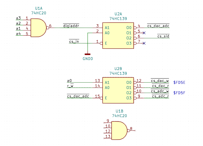
It's reusing the few connections I can clearly see on board pictures (a3 on pin 1 of U1 and U1 pin 6 to U2 pin 3).
On the pics I can also see something going out from pin 8 of U1 and under the SID, so there must either be something else (maybe one of the /cs's needs to be inverted?) or it's just using a different method.
|
|
Posted By
TLC
on 2022-11-11
04:22:06
| Re: Let's remake the DigiBlaster!
@SukkoPera it looks neat indeed. Re: inverting some signals, I seem to have an idea here. I think the ZN427 datasheet looks to have a typo, I mean it talks about an RD' (RD inverted) output enable strobe on the title page, but later it really shows a positive (non-inverted) one in the read timing diagram. That is, I guess the ZN427 appears to really need a positive read strobe, which seems to justify the need of inverting the cs_adc_r signal.
Also, I noticed that the ZN427 appears to need a clock signal for it's operation, that is, a <= 900kHz one (hint, hint...  ). Ed.: I mean, the hacked-together stable 50% single clock (which the SID card produces to feed the SID with) comes really handy here. It's just within specs. The same construct already wouldn't work in the C64 (or, a standard 985kHz-fed SID) at all. ). Ed.: I mean, the hacked-together stable 50% single clock (which the SID card produces to feed the SID with) comes really handy here. It's just within specs. The same construct already wouldn't work in the C64 (or, a standard 985kHz-fed SID) at all.
Yet another comment: I think the 1/2W resistor that you tagged R3 should probably be a small (discrete) inductor instead. I don't know if it really is of course, but... 1.) as you pointed out, the comparator inside the ZN427 needs a negative supply, which (the DC-DC converter, that is) may or may not require an inductor, but more often than not, it does; and 2.) apparently there's nothing in this circuit that'd justify a 1/2W resistor.
|
|
| |
Copyright © Plus/4 World Team, 2001-2025. Support Plus/4 World on Patreon |